SGLS118D December 2001 – September 2016
PRODUCTION DATA.
- 1 Features
- 2 Applications
- 3 Description
- 4 Revision History
- 5 Description (continued)
- 6 Pin Configuration and Functions
- 7 Specifications
- 8 Detailed Description
- 9 Application and Implementation
- 10Power Supply Recommendations
- 11Layout
- 12Device and Documentation Support
- 13Mechanical, Packaging, and Orderable Information
パッケージ・オプション
デバイスごとのパッケージ図は、PDF版データシートをご参照ください。
メカニカル・データ(パッケージ|ピン)
- DBV|5
サーマルパッド・メカニカル・データ
発注情報
9 Application and Implementation
NOTE
Information in the following applications sections is not part of the TI component specification, and TI does not warrant its accuracy or completeness. TI’s customers are responsible for determining suitability of components for their purposes. Customers should validate and test their design implementation to confirm system functionality.
9.1 Application Information
The TPS769xx-Q1 uses a PMOS pass element to dramatically reduce both dropout voltage and supply current over more conventional PNP-pass-element LDO designs. The PMOS pass element is a voltage-controlled device and, unlike a PNP transistor, it does not require increased drive current as output current increases. Supply current in the TPS769xx-Q1 is essentially constant from no load to maximum load.
Current limiting and thermal protection prevent damage by excessive output current and/or power dissipation. The device switches into a constant-current mode at approximately 350 mA; further load reduces the output voltage instead of increasing the output current. The thermal protection shuts the regulator off if the junction temperature rises above approximately 165°C. Recovery is automatic when the junction temperature drops approximately 25°C below the high temperature trip point. The PMOS pass element includes a back gate diode that conducts reverse current when the input voltage level drops below the output voltage level.
A voltage of 1.7 V or greater on the EN input disables the TPS769xx-Q1 internal circuitry, reducing the supply current to 1 µA. A voltage of less than 0.9 V on the EN input enables the TPS769xx and enables normal operation to resume. The EN input does not include any deliberate hysteresis, and it exhibits an actual switching threshold of approximately 1.5 V.
9.2 Typical Application

9.2.1 Design Requirements
Table 1 lists the design parameters for this example.
Table 1. Design Parameters
| PARAMETER | EXAMPLE VALUE |
|---|---|
| Input voltage range | 4 V to 10 V |
| Output voltage | 2.5 V to 5 V |
| Output current rating | 100 mA |
| Output capacitor | 4.7 µF to 10 µF |
| Output capacitor ESD range | 200 mΩ to 10 Ω |
9.2.2 Detailed Design Procedure
9.2.2.1 External Capacitor Requirements
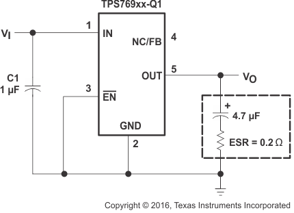
Although not required, TI recommends a 0.047-µF or larger ceramic input bypass capacitor, connected between IN and GND and located close to the TPS769xx-Q1, to improve transient response and noise rejection. A higher-value electrolytic input capacitor may be necessary if large, fast-rise-time load transients are anticipated and the device is located several inches from the power source.
Like all low dropout regulators, the TPS769xx-Q1 requires an output capacitor connected between OUT and GND to stabilize the internal control loop. The minimum recommended capacitance is 4.7 µF. The ESR (equivalent series resistance) of the capacitor must be between 0.2 Ω and 10 Ω. to ensure stability. Capacitor values larger than 4.7 µF are acceptable, and allow the use of smaller ESR values. Capacitances less than 4.7 µF are not recommended because they require careful selection of ESR to ensure stability. Solid tantalum electrolytic, aluminum electrolytic, and multilayer ceramic capacitors are all suitable, provided they meet the requirements described above. Most of the commercially available 4.7-µF surface-mount solid tantalum capacitors, including devices from Sprague, Kemet, and Nichico, meet the ESR requirements stated above. Multilayer ceramic capacitors may have very small equivalent series resistances and may therefore require the addition of a low value series resistor to ensure stability.
Table 2. Capacitor Selection
| PART NO. | MFR. | VALUE | MAX ESR | SIZE (H × L × W)(1) |
|---|---|---|---|---|
| T494B475K016AS | KEMET | 4.7 µF | 1.5 Ω | 1.9 × 3.5 × 2.8 |
| 195D106x0016x2T | SPRAGUE | 10 µF | 1.5 Ω | 1.3 × 7 × 2.7 |
| 695D106x003562T | SPRAGUE | 10 µF | 1.3 Ω | 2.5 × 7.6 × 2.5 |
| TPSC475K035R0600 | AVX | 4.7 µF | 0.6 Ω | 2.6 × 6 × 3.2 |
9.2.2.2 Output Voltage Programming
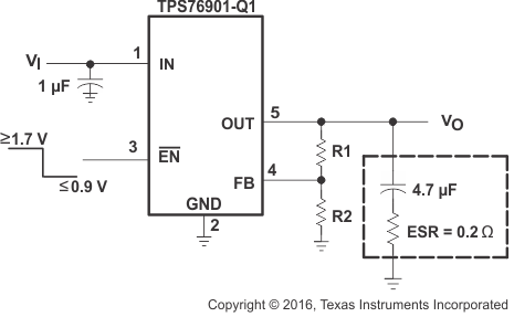
The output voltage of the TPS76901-Q1 adjustable regulator is programmed using an external resistor divider as shown in Figure 24. The output voltage is calculated using Equation 1.

where
- The internal reference voltage (VREF) = 1.224 V (typical)
Resistors R1 and R2 must be chosen for approximately 7-µA divider current. Lower value resistors can be used but offer no inherent advantage and waste more power. Higher values must be avoided as leakage currents at FB increase the output voltage error. The recommended design procedure is to choose R2 = 169 kΩ to set the divider current at 7 µA and then calculate R1 using Equation 2.

Table 3. Output Voltage Programming Guide
| OUTPUT VOLTAGE (V) | DIVIDER RESISTANCE (kΩ)(1) | |
|---|---|---|
| R1 | R2 | |
| 2.5 | 174 | 169 |
| 3.3 | 287 | 169 |
| 3.6 | 324 | 169 |
| 4 | 383 | 169 |
| 5 | 523 | 169 |
 Figure 24. TPS76901-Q1 Adjustable LDO Regulator Programming
9.2.3 Application Curves
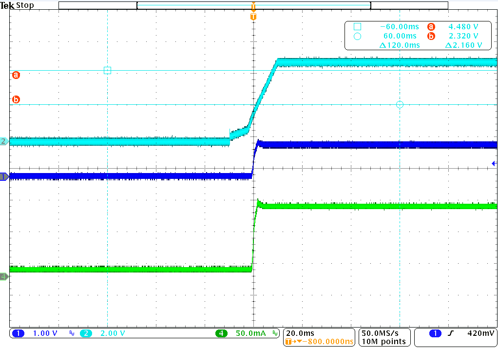
 Figure 25. Power-Up Waveform
(CH1 VOUT, CH2 VIN, CH4 IOUT)
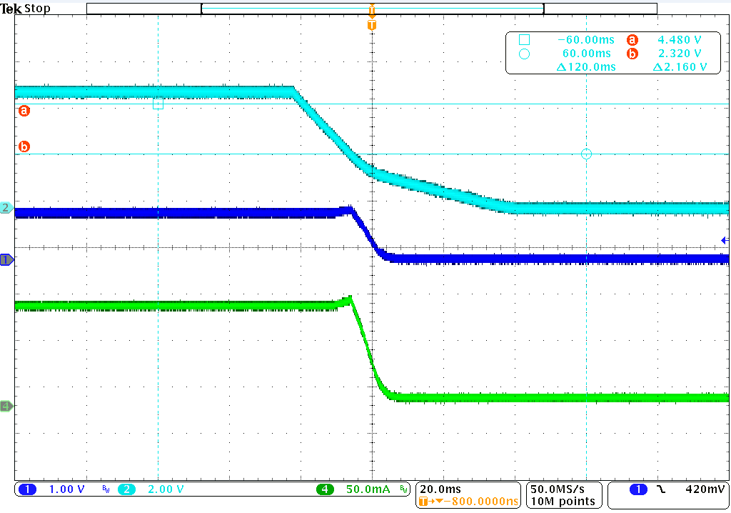
 Figure 26. Power-Down Waveform
(CH1 VOUT, CH2 VIN, CH4 IOUT)