JAJSG59B september 2018 – december 2020 TPS7A11
PRODUCTION DATA
- 1
- 1 特長
- 2 アプリケーション
- 3 説明
- 4 Revision History
- 5 Pin Configuration and Functions
- 6 Specifications
- 7 Detailed Description
-
8 Application and Implementation
- 8.1
Application Information
- 8.1.1 Recommended Capacitor Types
- 8.1.2 Input and Output Capacitor Requirements
- 8.1.3 Load Transient Response
- 8.1.4 Dropout Voltage
- 8.1.5 Behavior During Transition From Dropout Into Regulation
- 8.1.6 Undervoltage Lockout Circuit Operation
- 8.1.7 Power Dissipation (PD)
- 8.1.8 Estimating Junction Temperature
- 8.1.9 Recommended Area for Continuous Operation
- 8.2 Typical Application
- 8.1
Application Information
- 9 Power Supply Recommendations
- 10Layout
- 11Device and Documentation Support
- Mechanical, Packaging, and Orderable Information
パッケージ・オプション
メカニカル・データ(パッケージ|ピン)
サーマルパッド・メカニカル・データ
- DRV|6
発注情報
8.1.3 Load Transient Response
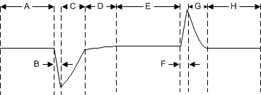
The load-step transient response is the output voltage response by the LDO to a step in load current while output voltage regulation is maintained. See Figure 6-20 to Figure 6-23 for typical load transient response. There are two key transitions during a load transient response: the transition from a light to a heavy load, and the transition from a heavy to a light load. The regions in Figure 8-1 are broken down as described in this section. Regions A, E, and H are where the output voltage is in steady-state operation.
 Figure 8-1 Load Transient Waveform
During transitions from a light load to a heavy load, the:
- Initial voltage dip is a result of the depletion of the output capacitor charge and parasitic impedance to the output capacitor (region B)
- Recovery from the dip results from the LDO increasing the sourcing current, and leads to output voltage regulation (region C)
During transitions from a heavy load to a light load, the:
- Initial voltage rise results from the LDO sourcing a large current, and leads to an increase in the output capacitor charge (region F)
- Recovery from the rise results from the LDO decreasing its sourcing current in combination with the load discharging the output capacitor (region G)
A larger output capacitance reduces the peaks during a load transient but slows down the response time of the device. A larger dc load also reduces the peaks because the amplitude of the transition is lowered and a higher current discharge path is provided for the output capacitor.