JAJSCI9A May 2016 – September 2016 TPS7A19
PRODUCTION DATA.
- 1 特長
- 2 アプリケーション
- 3 概要
- 4 改訂履歴
- 5 Pin Configuration and Functions
- 6 Specifications
- 7 Detailed Description
- 8 Application and Implementation
- 9 Power Supply Recommendations
- 10Layout
- 11デバイスおよびドキュメントのサポート
- 12メカニカル、パッケージ、および注文情報
パッケージ・オプション
メカニカル・データ(パッケージ|ピン)
- DRB|8
サーマルパッド・メカニカル・データ
- DRB|8
発注情報
10 Layout
10.1 Layout Guidelines
- To improve ac performance such as PSRR, output noise, and transient response, design the board with separate ground planes for VIN and VOUT, with each ground plane connected only at the GND pin of the device. In addition, connect the ground connection for the output capacitor directly to the GND pin of the device.
- Minimize equivalent series inductance (ESL) and equivalent series resistance (ESR) in order to maximize performance and stability. Place every capacitor as close to the device as possible, and on the same side of the PCB as the regulator.
- Do not place any of the capacitors on the opposite side of the PCB from where the regulator is installed. The use of vias and long traces are strongly discouraged because of the negative impact on system performance. Vias and long traces can also cause instability.
- If possible, and to maximize the performance listed in this data sheet, use the same layout pattern used for the TPS7A19 evaluation module, TPS7A1901EVM-760 (SBVU031).
10.2 Layout Example
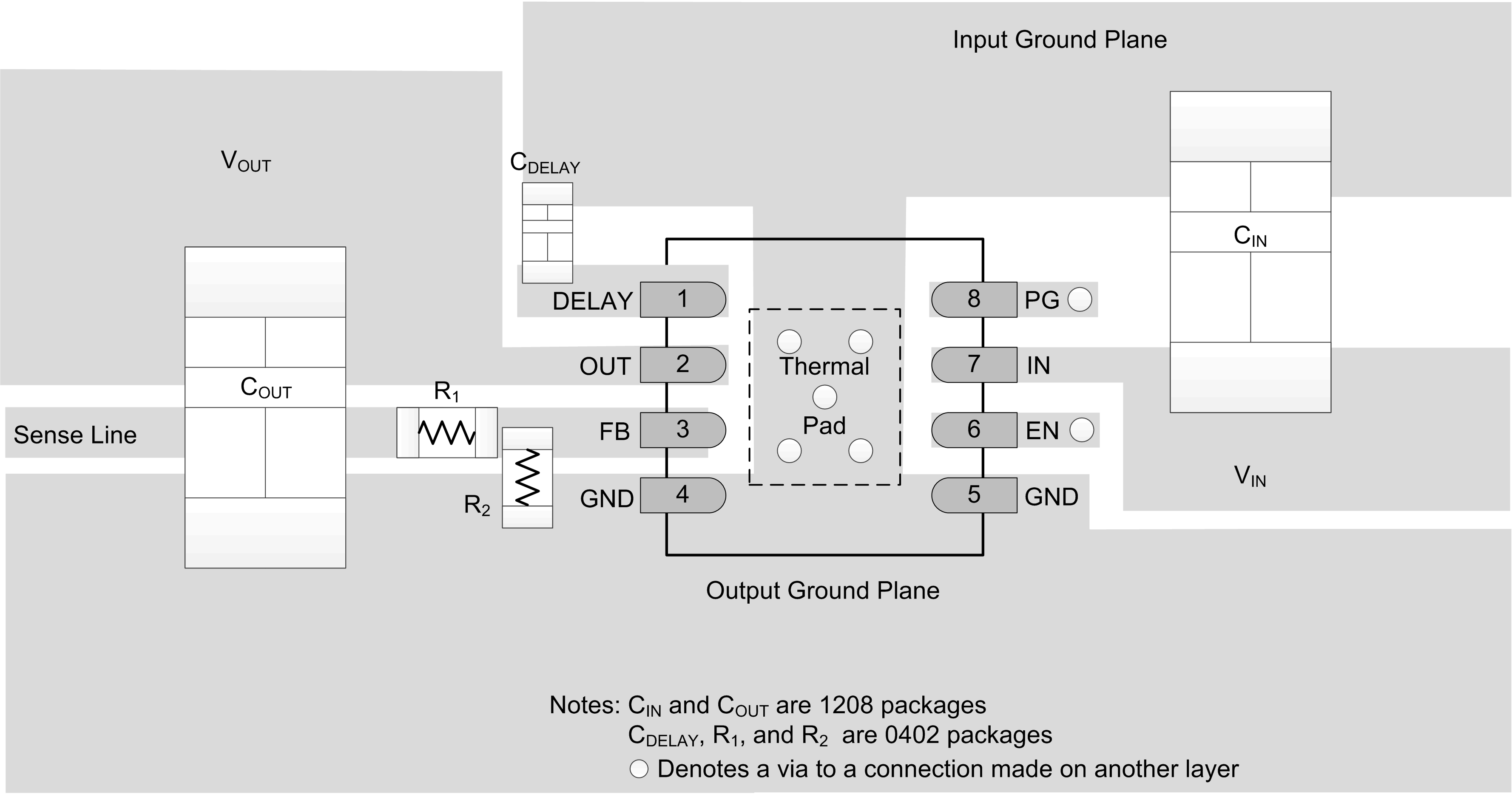 Figure 16. TPS7A19 Layout Example