JAJSPA7A November   2022  – December 2022 TPS7A53A-Q1

PRODUCTION DATA  

  1. 特長
  2. アプリケーション
  3. 概要
  4. Revision History
  5. Pin Configuration and Functions
  6. Specifications
    1. 6.1 Absolute Maximum Ratings
    2. 6.2 ESD Ratings
    3. 6.3 Recommended Operating Conditions
    4. 6.4 Thermal Information
    5. 6.5 Electrical Characteristics
    6. 6.6 Typical Characteristics
  7. Detailed Description
    1. 7.1 Overview
    2. 7.2 Functional Block Diagram
    3. 7.3 Feature Description
      1. 7.3.1 Enable and Shutdown
      2. 7.3.2 Active Discharge
      3. 7.3.3 Power-Good Output (PG)
      4. 7.3.4 Internal Current Limit
      5. 7.3.5 Thermal Shutdown Protection (TSD)
    4. 7.4 Device Functional Modes
      1. 7.4.1 Normal Operation
      2. 7.4.2 Dropout Operation
      3. 7.4.3 Disabled
  8. Application and Implementation
    1. 8.1 Application Information
      1. 8.1.1 Input, Output, and Bias Capacitor Requirements
      2. 8.1.2 Dropout Voltage
      3. 8.1.3 Output Noise
      4. 8.1.4 Estimating Junction Temperature
      5. 8.1.5 Soft Start, Sequencing, and Inrush Current
      6. 8.1.6 Power-Good Operation
    2. 8.2 Typical Application
      1. 8.2.1 Design Requirements
      2. 8.2.2 Detailed Design Procedure
      3. 8.2.3 Application Curve
    3. 8.3 Power Supply Recommendations
    4. 8.4 Layout
      1. 8.4.1 Layout Guidelines
        1. 8.4.1.1 Board Layout
        2. 8.4.1.2 RTJ Package — High CTE Mold Compound
      2. 8.4.2 Layout Example
  9. Device and Documentation Support
    1. 9.1 Documentation Support
      1. 9.1.1 Related Documentation
    2. 9.2 Receiving Notification of Documentation Updates
    3. 9.3 サポート・リソース
    4. 9.4 Trademarks
    5. 9.5 Electrostatic Discharge Caution
    6. 9.6 Glossary
  10. 10Mechanical, Packaging, and Orderable Information
    1. 10.1 Mechanical Data

パッケージ・オプション

メカニカル・データ(パッケージ|ピン)
サーマルパッド・メカニカル・データ
発注情報

Power-Good Output (PG)

The PG signal provides an easy solution to meet demanding sequencing requirements because PG signals when the output nears the nominal value. PG can be used to signal other devices in a system when the output voltage is near, at, or above the set output voltage (VOUT(nom)). Figure 7-1 shows a simplified schematic.

The PG signal is an open-drain digital output that requires a pullup resistor to a voltage source and is active high. The PG circuit sets the PG pin into a high-impedance state to indicate that the power is good.

Using a large feed-forward capacitor (CFF) delays the output voltage and, because the PG circuit monitors the FB pin, the PG signal can indicate a false positive.
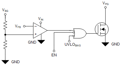
GUID-20221201-SS0I-LCNG-7LH0-80PZSDXXZNXK-low.gif Figure 7-1 Simplified PG Circuit