JAJSQ32A August   2023  – January 2024 TPS7A53B

PRODUCTION DATA  

  1.   1
  2. 特長
  3. アプリケーション
  4. 概要
  5. Pin Configuration and Functions
  6. Specifications
    1. 5.1 Absolute Maximum Ratings
    2. 5.2 ESD Ratings
    3. 5.3 Recommended Operating Conditions
    4. 5.4 Thermal Information
    5. 5.5 Electrical Characteristics
    6. 5.6 Typical Characteristics
  7. Detailed Description
    1. 6.1 Overview
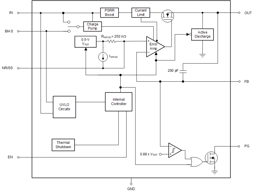
    2. 6.2 Functional Block Diagram
    3. 6.3 Feature Description
      1. 6.3.1 Voltage Regulation Features
        1. 6.3.1.1 DC Regulation
        2. 6.3.1.2 AC and Transient Response
      2. 6.3.2 System Start-Up Features
        1. 6.3.2.1 Programmable Soft-Start (NR/SS Pin)
        2. 6.3.2.2 Internal Sequencing
          1. 6.3.2.2.1 Enable (EN)
          2. 6.3.2.2.2 Undervoltage Lockout (UVLO) Control
          3. 6.3.2.2.3 Active Discharge
        3. 6.3.2.3 Power-Good Output (PG)
      3. 6.3.3 Internal Protection Features
        1. 6.3.3.1 Foldback Current Limit (ICL)
        2. 6.3.3.2 Thermal Protection (Tsd)
    4. 6.4 Device Functional Modes
      1. 6.4.1 Regulation
      2. 6.4.2 Disabled
      3. 6.4.3 Current Limit Operation
  8. Application and Implementation
    1. 7.1 Application Information
      1. 7.1.1  Recommended Capacitor Types
        1. 7.1.1.1 Input and Output Capacitor Requirements (CIN and COUT)
        2. 7.1.1.2 Noise-Reduction and Soft-Start Capacitor (CNR/SS)
        3. 7.1.1.3 Feed-Forward Capacitor (CFF)
      2. 7.1.2  Soft-Start and Inrush Current
      3. 7.1.3  Optimizing Noise and PSRR
      4. 7.1.4  Charge Pump Noise
      5. 7.1.5  Current Sharing
      6. 7.1.6  Adjustable Operation
      7. 7.1.7  Power-Good Operation
      8. 7.1.8  Undervoltage Lockout (UVLO) Operation
      9. 7.1.9  Dropout Voltage (VDO)
      10. 7.1.10 Device Behavior During Transition From Dropout Into Regulation
      11. 7.1.11 Load Transient Response
      12. 7.1.12 Reverse Current Protection Considerations
      13. 7.1.13 Power Dissipation (PD)
      14. 7.1.14 Estimating Junction Temperature
      15. 7.1.15 TPS7A53EVM Thermal Analysis
    2. 7.2 Typical Application
      1. 7.2.1 Design Requirements
      2. 7.2.2 Detailed Design Procedure
      3. 7.2.3 Application Curves
    3. 7.3 Power Supply Recommendations
    4. 7.4 Layout
      1. 7.4.1 Layout Guidelines
        1. 7.4.1.1 Board Layout
      2. 7.4.2 Layout Example
  9. Device and Documentation Support
    1. 8.1 Device Support
      1. 8.1.1 Device Nomenclature
    2. 8.2 Documentation Support
      1. 8.2.1 Related Documentation
    3. 8.3 ドキュメントの更新通知を受け取る方法
    4. 8.4 サポート・リソース
    5. 8.5 Trademarks
    6. 8.6 静電気放電に関する注意事項
    7. 8.7 用語集
  10. Revision History
  11. 10Mechanical, Packaging, and Orderable Information

パッケージ・オプション

メカニカル・データ(パッケージ|ピン)
サーマルパッド・メカニカル・データ
発注情報

Functional Block Diagram

GUID-20230405-SS0I-JWJM-J9V6-HJL4WNGH15ZV-low.gif