JAJSDB7B June   2017  – October 2021 TPS7A83A

PRODUCTION DATA  

  1. 特長
  2. アプリケーション
  3. 概要
  4. Revision History
  5. 概要 (続き)
  6. Pin Configuration and Functions
  7. Specifications
    1. 7.1 Absolute Maximum Ratings
    2. 7.2 ESD Ratings
    3. 7.3 Recommended Operating Conditions
    4. 7.4 Thermal Information
    5. 7.5 Electrical Characteristics: General
    6. 7.6 Electrical Characteristics: TPS7A8300A
    7. 7.7 Electrical Characteristics: TPS7A8301A
    8. 7.8 Typical Characteristics: TPS7A8300A
    9. 7.9 Typical Characteristics: TPS7A8301A
  8. Detailed Description
    1. 8.1 Overview
    2. 8.2 Functional Block Diagram
    3. 8.3 Feature Description
      1. 8.3.1 Voltage Regulation Features
        1. 8.3.1.1 DC Regulation
        2. 8.3.1.2 AC and Transient Response
      2. 8.3.2 System Start-Up Features
        1. 8.3.2.1 Programmable Soft-Start (NR/SS)
        2. 8.3.2.2 Internal Sequencing
          1. 8.3.2.2.1 Enable (EN)
          2. 8.3.2.2.2 Undervoltage Lockout (UVLO) Control
          3. 8.3.2.2.3 Active Discharge
        3. 8.3.2.3 Power-Good Output (PG)
      3. 8.3.3 Internal Protection Features
        1. 8.3.3.1 Foldback Current Limit (ICL)
        2. 8.3.3.2 Thermal Protection (Tsd)
    4. 8.4 Device Functional Modes
      1. 8.4.1 Regulation
      2. 8.4.2 Disabled
  9. Application and Implementation
    1. 9.1 Application Information
      1. 9.1.1 External Component Selection
        1. 9.1.1.1 Adjustable Operation
        2. 9.1.1.2 ANY-OUT Programmable Output Voltage
        3. 9.1.1.3 ANY-OUT Operation
        4. 9.1.1.4 Increasing ANY-OUT Resolution for LILO Conditions
        5. 9.1.1.5 Recommended Capacitor Types
        6. 9.1.1.6 Input and Output Capacitor Requirements (CIN and COUT)
        7. 9.1.1.7 Feed-Forward Capacitor (CFF)
        8. 9.1.1.8 Noise-Reduction and Soft-Start Capacitor (CNR/SS)
      2. 9.1.2 Start Up
        1. 9.1.2.1 Soft-Start (NR/SS)
          1. 9.1.2.1.1 Inrush Current
        2. 9.1.2.2 Undervoltage Lockout (UVLO)
        3. 9.1.2.3 Power-Good (PG) Function
      3. 9.1.3 AC and Transient Performance
        1. 9.1.3.1 Power-Supply Rejection Ratio (PSRR)
        2. 9.1.3.2 Output Voltage Noise
        3. 9.1.3.3 Optimizing Noise and PSRR
          1. 9.1.3.3.1 Charge Pump Noise
        4. 9.1.3.4 Load Transient Response
      4. 9.1.4 DC Performance
        1. 9.1.4.1 Output Voltage Accuracy (VOUT)
        2. 9.1.4.2 Dropout Voltage (VDO)
          1. 9.1.4.2.1 Behavior When Transitioning From Dropout Into Regulation
      5. 9.1.5 Sequencing Requirements
      6. 9.1.6 Negatively Biased Output
      7. 9.1.7 Reverse Current
      8. 9.1.8 Power Dissipation (PD)
        1. 9.1.8.1 Estimating Junction Temperature
        2. 9.1.8.2 Recommended Area for Continuous Operation (RACO)
    2. 9.2 Typical Application
      1. 9.2.1 Design Requirements
      2. 9.2.2 Detailed Design Procedure
      3. 9.2.3 Application Curves
  10. 10Power Supply Recommendations
  11. 11Layout
    1. 11.1 Layout Guidelines
    2. 11.2 Layout Example
  12. 12Device and Documentation Support
    1. 12.1 Device Support
      1. 12.1.1 Development Support
        1. 12.1.1.1 Evaluation Models
        2. 12.1.1.2 Spice Models
      2. 12.1.2 Device Nomenclature
    2. 12.2 Documentation Support
      1. 12.2.1 Related Documentation
    3. 12.3 Receiving Notification of Documentation Updates
    4. 12.4 サポート・リソース
    5. 12.5 Trademarks
    6. 12.6 Electrostatic Discharge Caution
    7. 12.7 Glossary
  13. 13Mechanical, Packaging, and Orderable Information

パッケージ・オプション

メカニカル・データ(パッケージ|ピン)
サーマルパッド・メカニカル・データ
発注情報

Typical Characteristics: TPS7A8301A

at TA = 25°C, VIN = 1.4 V or VIN = VOUT(nom) + 0.3 V (whichever is greater), VBIAS = open, VOUT(nom) = 0.8 V, VEN = 1.1 V, CIN = 10 μF, COUT = 22 μF, CNR/SS = 0 nF, CFF = 0 nF, and PG pin pulled up to VIN with 100 kΩ (unless otherwise noted)
GUID-20210923-SS0I-TKFR-63FM-CZSWNV2QKDMQ-low.png
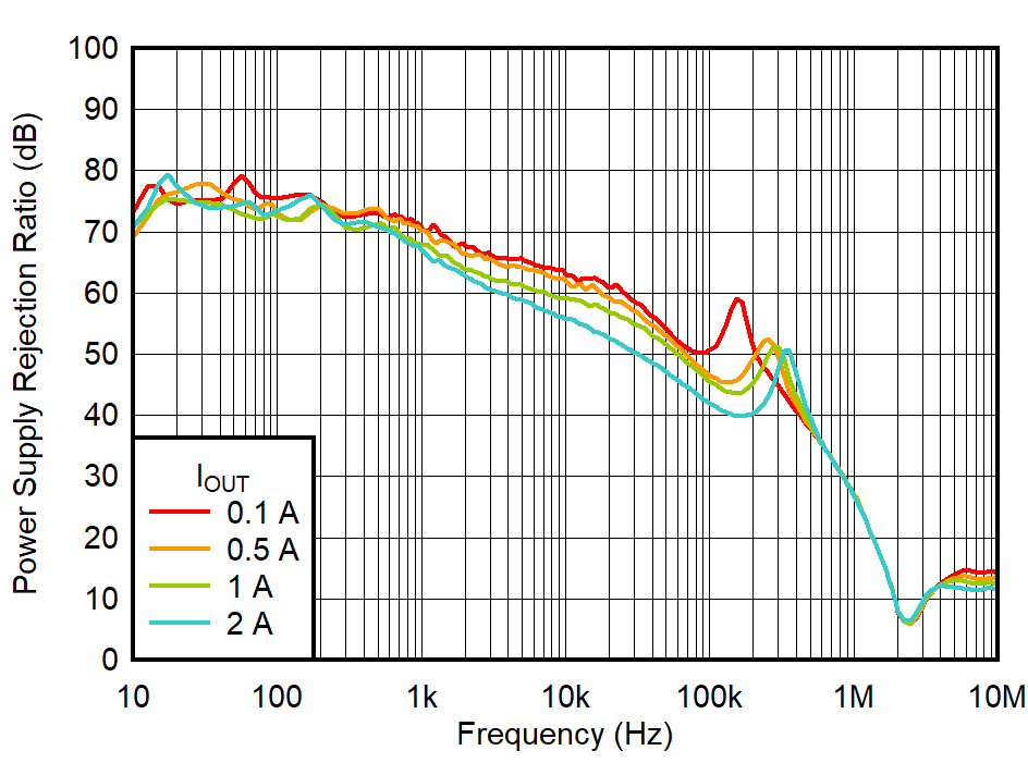
VIN = 1.1 V, VBIAS = 5 V, COUT = 22 μF, CNR/SS = 10 nF,
CFF = 10 nF
Figure 7-43 PSRR vs Frequency and IOUT
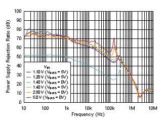
GUID-17DAABC1-237E-4110-88BF-CE5FAA9369A4-low.gif
IOUT = 1 A, COUT = 22 μF, CNR/SS = 10 nF, CFF = 10 nF
 
Figure 7-45 PSRR vs Frequency and VIN
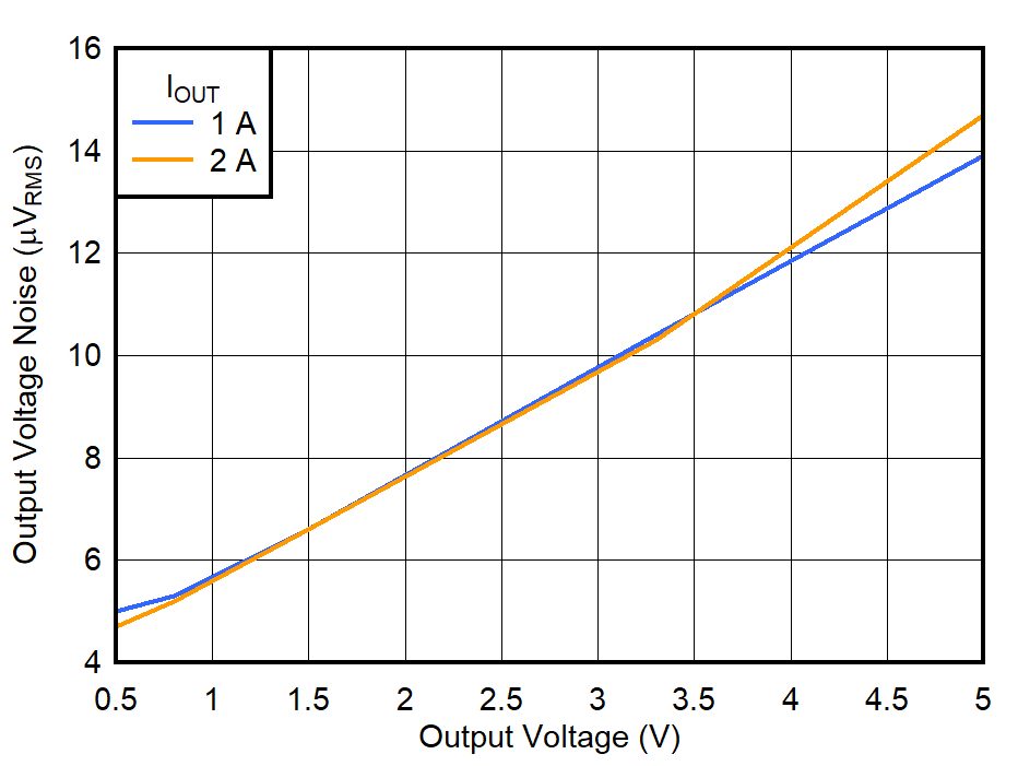
GUID-20210923-SS0I-0C15-1RHJ-DQBLNLS0WSBB-low.png
VIN = VOUT + 0.3 V or VIN = 1.1 V (whichever is greater) and VBIAS = 5 V for VOUT ≤ 2.2 V,
COUT = 47 μF || 10μF || 10μF, CNR/SS = 10 nF, CFF = 10 nF, RMS noise BW = 10 Hz to 100 kHz
Figure 7-47 Output Voltage Noise vs VOUT
GUID-2412B56F-6DD9-4D78-9E60-DAA5B2EECD70-low.gif
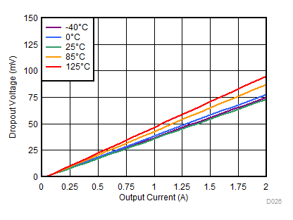
VIN = 1.1 V, VBIAS = 3 V
Figure 7-49 Dropout Voltage vs Output Current With BIAS
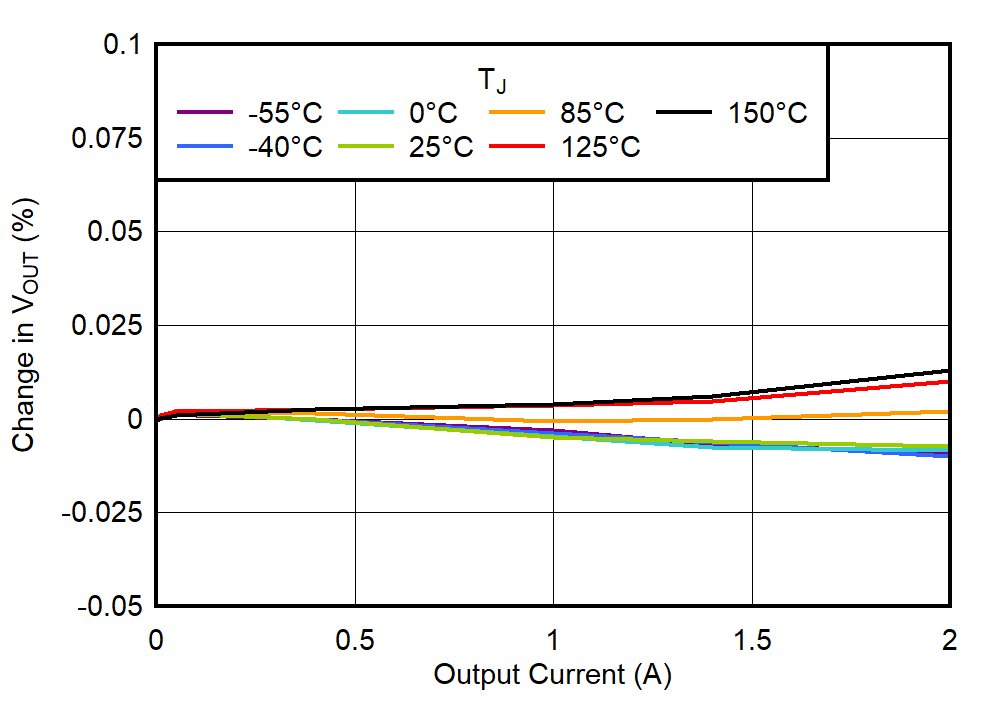
GUID-20210923-SS0I-KHTN-VQRQ-ZBQ56TCKKHFX-low.png
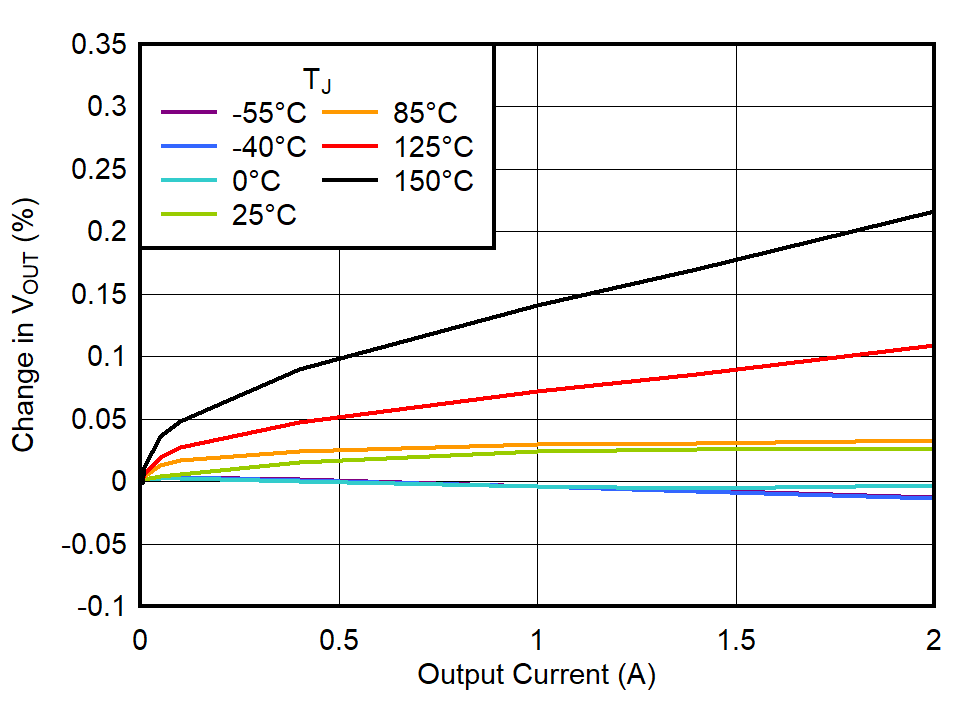
VIN = 1.4 V
Figure 7-51 Load Regulation
GUID-20210923-SS0I-DTBS-XGVL-XWGCBBKLQ9ZP-low.png
VIN = 5.55 V, VOUT = 5.15 V
Figure 7-53 Load Regulation (5-V Output)
GUID-62BF2410-9777-4E40-9381-A16E0B3CBA3C-low.gif
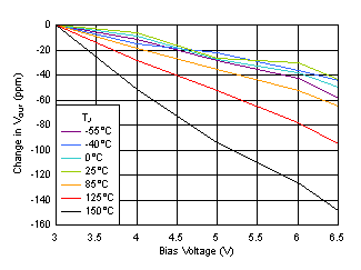
VOUT = 0.5 V, VIN = 1.1 V, IOUT = 5 mA, VBIAS = 5 V
Figure 7-55 Line Regulation With BIAS
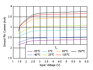
GUID-9EB84AD4-7EAD-4630-A95F-68857B0A9928-low.gif
VBIAS = 0 V, IOUT = 5 mA
Figure 7-57 Ground Pin Current vs Input Voltage
GUID-F369BDDD-8F55-4308-B5D3-31896706903F-low.gif
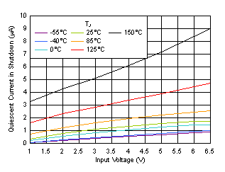
VBIAS = 0 V
Figure 7-59 Shutdown Current vs Input Voltage
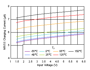
GUID-BB3901A3-FFAB-450B-8417-B2C9D7309A32-low.gif
VBIAS = 0 V
Figure 7-61 INR/SS Current vs Input Voltage
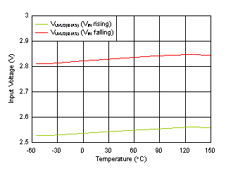
GUID-20913F17-094A-43C5-AAE2-7065EA12A1C6-low.gif
VIN = 1.1 V
Figure 7-63 VBIAS UVLO vs Temperature
GUID-4E30CC22-3279-4A15-8D64-57CE5166DCEE-low.gif
 
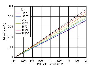
Figure 7-65 PG Voltage vs PG Current Sink
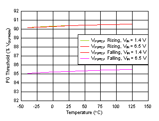
GUID-15FE8F1C-08A4-4924-A923-3989FED57C11-low.gif
 
Figure 7-67 PG Threshold vs Temperature
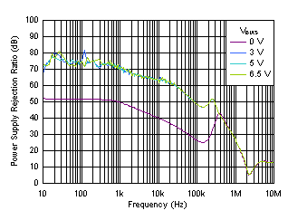
GUID-AB2A3807-DAC1-4263-9C30-E20527FF8F6D-low.gif
VIN = 1.4 V, IOUT = 1 A, COUT = 22 μF, CNR/SS = 10 nF,
CFF = 10 nF
Figure 7-44 PSRR vs Frequency and VBIAS
GUID-20210923-SS0I-XCLG-CW3P-D6TT2GVB8VMS-low.png
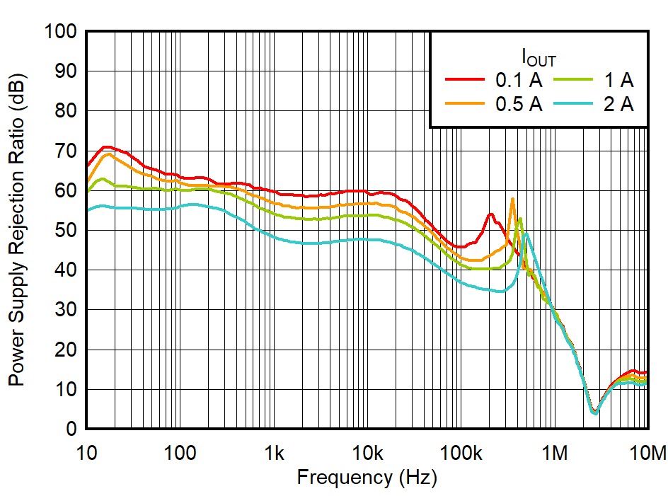
VIN = 5.5 V, VOUT = 5 V, COUT = 47 μF || 10 μF || 10μF,
CNR/SS = 10 nF, CFF = 10 nF
Figure 7-46 PSRR vs Frequency and IOUT (VOUT = 5 V)
GUID-3F5F3A23-6436-4534-9250-DB1694270ED3-low.gif
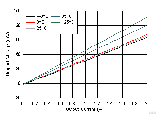
VIN = 1.4 V


Figure 7-48 Dropout Voltage vs Output Current Without BIAS
GUID-A2FDCEC9-FFCD-4595-893C-34C8EC1B6E2B-low.gif
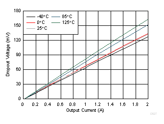
VIN = 5.5 V
Figure 7-50 Dropout Voltage vs Output Current (High VIN)
GUID-20210923-SS0I-NCFV-FVJR-D1DHGBVDS289-low.png
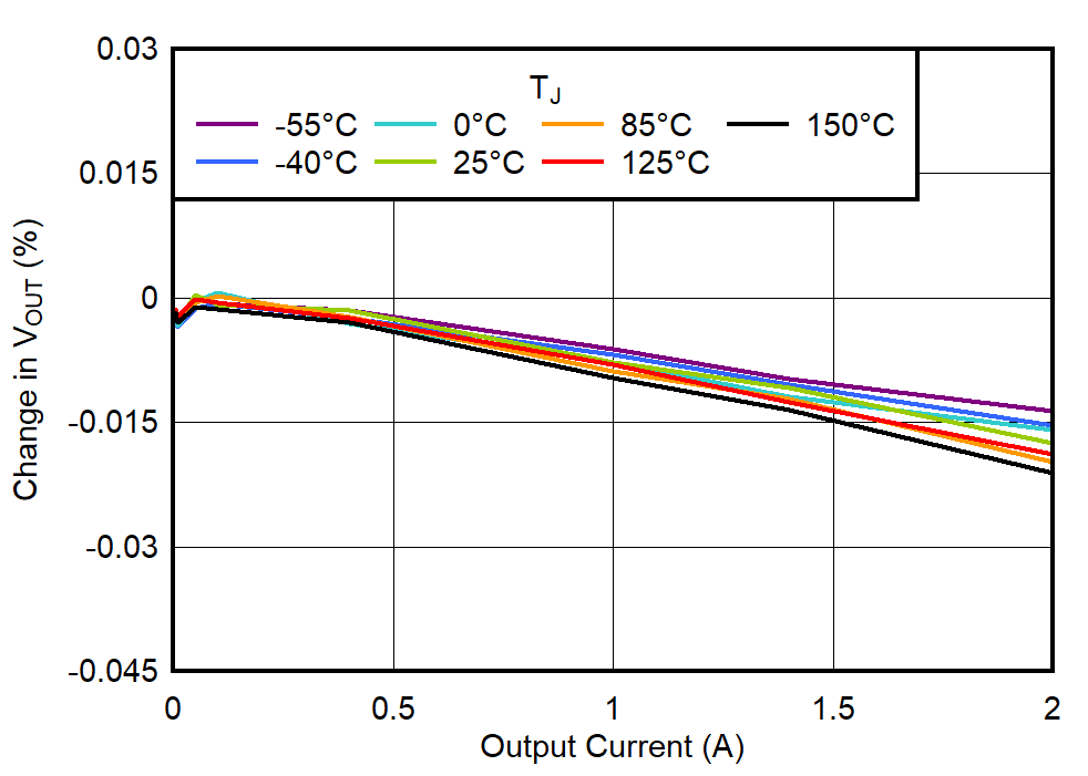
VIN = 3.8 V
Figure 7-52 Load Regulation (3.3-V Output)
GUID-B7CCED47-B84E-418E-A253-B050B99A72CE-low.gif
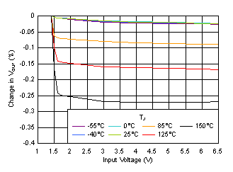
VOUT = 0.5 V, IOUT = 5 mA
 
Figure 7-54 Line Regulation vs VIN
GUID-E1F12F88-E9B4-4E3A-97AB-57443F33D227-low.gif
IOUT = 5 mA
Figure 7-56 Line Regulation vs VIN (5.2-V Output)
GUID-2F919B36-3D8E-4788-9056-F3EC212D1373-low.gif
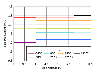
VIN = 1.1 V, IOUT = 5 mA
Figure 7-58 BIAS Pin Current vs Bias Voltage
GUID-517FA019-AA21-4026-B956-066F9BE31EF2-low.gif
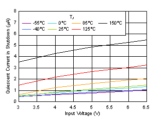
VIN = 1.1 V
Figure 7-60 Shutdown Current vs Bias Voltage
GUID-8677CCB6-0751-44CA-B665-4EE45EFAC501-low.gif
 
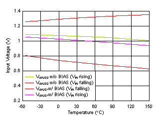
Figure 7-62 VIN UVLO vs Temperature
GUID-A1176A7B-2AB5-48DD-BB45-7D32CAACCA37-low.gif
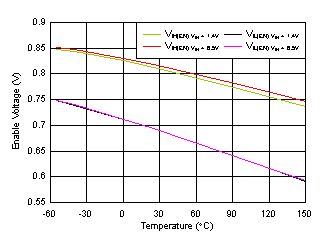
VIN = 1.4 V, 6.5 V
Figure 7-64 Enable Threshold vs Temperature
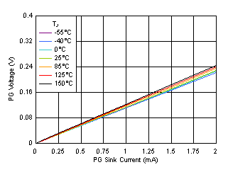
GUID-C504C26F-3A9D-41D0-BC65-FF8C0F5B890B-low.gif
VIN = 6.5 V
Figure 7-66 PG Voltage vs PG Current Sink