JAJSDB7B June 2017 – October 2021 TPS7A83A
PRODUCTION DATA
- 1 特長
- 2 アプリケーション
- 3 概要
- 4 Revision History
- 5 概要 (続き)
- 6 Pin Configuration and Functions
-
7 Specifications
- 7.1 Absolute Maximum Ratings
- 7.2 ESD Ratings
- 7.3 Recommended Operating Conditions
- 7.4 Thermal Information
- 7.5 Electrical Characteristics: General
- 7.6 Electrical Characteristics: TPS7A8300A
- 7.7 Electrical Characteristics: TPS7A8301A
- 7.8 Typical Characteristics: TPS7A8300A
- 7.9 Typical Characteristics: TPS7A8301A
- 8 Detailed Description
-
9 Application and Implementation
- 9.1
Application Information
- 9.1.1
External Component Selection
- 9.1.1.1 Adjustable Operation
- 9.1.1.2 ANY-OUT Programmable Output Voltage
- 9.1.1.3 ANY-OUT Operation
- 9.1.1.4 Increasing ANY-OUT Resolution for LILO Conditions
- 9.1.1.5 Recommended Capacitor Types
- 9.1.1.6 Input and Output Capacitor Requirements (CIN and COUT)
- 9.1.1.7 Feed-Forward Capacitor (CFF)
- 9.1.1.8 Noise-Reduction and Soft-Start Capacitor (CNR/SS)
- 9.1.2 Start Up
- 9.1.3 AC and Transient Performance
- 9.1.4 DC Performance
- 9.1.5 Sequencing Requirements
- 9.1.6 Negatively Biased Output
- 9.1.7 Reverse Current
- 9.1.8 Power Dissipation (PD)
- 9.1.1
External Component Selection
- 9.2 Typical Application
- 9.1
Application Information
- 10Power Supply Recommendations
- 11Layout
- 12Device and Documentation Support
- 13Mechanical, Packaging, and Orderable Information
パッケージ・オプション
メカニカル・データ(パッケージ|ピン)
サーマルパッド・メカニカル・データ
発注情報
9.1.2.3 Power-Good (PG) Function
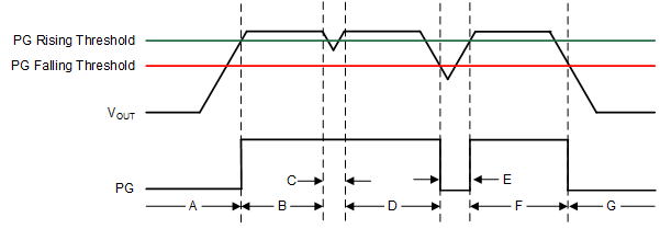
The PG circuit monitors the voltage at the feedback pin to indicate the status of the output voltage. The PG circuit asserts whenever FB, VIN, or EN are below their thresholds. Figure 9-5 and Table 9-6 describe the PG operation versus the output voltage.
 Figure 9-5 Typical PG Operation
| REGION | EVENT | PG STATUS | FB VOLTAGE |
|---|---|---|---|
| A | Turnon | 0 | VFB < VIT(PG) + VHYS(PG) |
| B | Regulation | Hi-Z | VFB ≥ VIT(PG) |
| C | Output voltage dip | Hi-Z | |
| D | Regulation | Hi-Z | |
| E | Output voltage dip | 0 | VFB < VIT(PG) |
| F | Regulation | Hi-Z | VFB ≥ VIT(PG) |
| G | Turnoff | 0 | VFB < VIT(PG) |
The PG pin is open-drain, and connecting a pullup resistor to an external supply enables others devices to receive power-good as a logic signal that can be used for sequencing. Make sure that the external pullup supply voltage results in a valid logic signal for the receiving device or devices.
To ensure proper operation of the PG circuit, the pullup resistor value must be from 10 kΩ and 100 kΩ. The lower limit of 10 kΩ results from the maximum pulldown strength of the PG transistor, and the upper limit of 100 kΩ results from the maximum leakage current at the PG node. If the pullup resistor is outside of this range, then the PG signal may not read a valid digital logic level.
Using a large CFF with a small CNR/SS causes the PG signal to incorrectly indicate that the output voltage has settled during turnon. The CFF time constant must be greater than the soft-start time constant to ensure proper operation of the PG during start-up. For a detailed description, see the Pros and Cons of Using a Feed-Forward Capacitor with a Low Dropout Regulator application report.
The state of PG is only valid when the device operates above the minimum supply voltage. During short brownout events and at light loads, PG does not assert because the output voltage (therefore VFB) is sustained by the output capacitance.