JAJSMS4F August 2021 – March 2024 TPS7H2211-SEP , TPS7H2211-SP
PRODUCTION DATA
- 1
- 1 特長
- 2 アプリケーション
- 3 概要
- 4 Device Options
- 5 Related Products
- 6 Pin Configuration and Functions
-
7 Specifications
- 7.1 Absolute Maximum Ratings
- 7.2 ESD Ratings
- 7.3 Recommended Operating Conditions
- 7.4 Thermal Information
- 7.5 Electrical Characteristics: All Devices
- 7.6 Electrical Characteristics: CFP and KGD Options
- 7.7 Electrical Characteristics: HTSSOP Option
- 7.8 Switching Characteristics: All Devices
- 7.9 Quality Conformance Inspection
- 7.10 Typical Characteristics
- 8 Parameter Measurement Information
- 9 Detailed Description
- 10Application and Implementation
- 11Device and Documentation Support
- 12Revision History
- 13Mechanical, Packaging, and Orderable Information
パッケージ・オプション
デバイスごとのパッケージ図は、PDF版データシートをご参照ください。
メカニカル・データ(パッケージ|ピン)
- DAP|32
- KGD|0
- HKR|16
サーマルパッド・メカニカル・データ
- DAP|32
発注情報
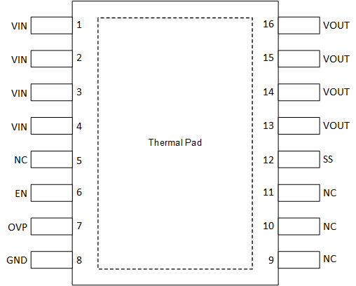
6 Pin Configuration and Functions
| HKR Package | DAP Package |
| 16-Pin CFP With Thermal Pad | 32-Pin HTSSOP With Thermal Pad |
| Top View | Top View |
 |
 |
Table 6-1 Pin Functions
| PIN | I/O(1) | DESCRIPTION | ||
|---|---|---|---|---|
| HKR (16) NO. | PW(32) NO. | NAME | ||
| 1-4 | 1-10 | VIN | I | Switch input. An input bypass capacitor is recommended for minimizing VIN dip. |
| 6 | 12 | EN | I | Active high switch control input. Do not float this pin. |
| 7 | 13 | OVP | I | Overvoltage protection. Set using an external resistor divider. If no OVP is desired, connect this pin to GND. Do not float this pin. |
| 8 | 15 | GND | — | Device ground. (2) |
| 12 | 22 | SS | I/O | Soft start (switch slew rate control). If this functionality is not desired, the SS pin must be left disconnected (floating). In all cases be sure to follow the requirements of Section 9.3.3. |
| 13-16 | 23-32 | VOUT | O | Switch output. A minimum 10-µF output capacitor is recommended. |
| 5, 9-11 | 11,14,16,17-21 | NC | — | NC — No connect. These pins are not internally connected. It is recommended to connect these pins to GND to prevent charge buildup; however, these pins can also be left open or tied to any voltage between GND and VIN. |
| — | Thermal Pad | — | Thermal pad (exposed center pad) for heat dissipation purposes. The thermal pad is internally connected to the seal ring and GND. | |
| — | Metal Lid | — | The lid is internally connected to the thermal pad and GND through the seal ring. | |
- I = Input, O = Output, I/O = Input or Output, — = Other
- Thermal pad is internally connected to the seal ring and GND for HKR option.
Table 6-2 Bare Die Information
| DIE THICKNESS | BACKSIDE FINISH | BACKSIDE POTENTIAL | BOND PAD METALLIZATION COMPOSITION | BOND PAD THICKNESS |
|---|---|---|---|---|
| 15 mils | Silicon with backgrind | Ground | AlCu | 1050 nm |

- All dimensions in microns (μm).
- The inner rectangle is the die and the outer rectangle is the die plus scribe lines.
Table 6-3 Bond Pad Coordinates in
Microns (μm)
| DESCRIPTION | PAD NUMBER | X MIN | Y MIN | X MAX | Y MAX |
|---|---|---|---|---|---|
| VIN | 1 | 653.22 | 4936.95 | 793.17 | 5076.9 |
| VIN | 2 | 152.37 | 4936.95 | 292.32 | 5076.9 |
| VIN | 3 | 319.32 | 4936.95 | 459.27 | 5076.9 |
| VIN | 4 | 486.27 | 4936.95 | 626.22 | 5076.9 |
| VIN | 5 | 152.37 | 4770 | 292.32 | 4909.95 |
| VIN | 6 | 319.32 | 4770 | 459.27 | 4909.95 |
| VIN | 7 | 486.27 | 4770 | 626.22 | 4909.95 |
| VIN | 8 | 653.22 | 4770 | 793.17 | 4909.95 |
| VIN | 9 | 152.37 | 4579.16 | 292.32 | 4719.11 |
| VIN | 10 | 319.32 | 4579.16 | 459.27 | 4719.11 |
| VIN | 11 | 486.27 | 4579.16 | 626.22 | 4719.11 |
| VIN | 12 | 653.22 | 4579.16 | 793.17 | 4719.11 |
| VIN | 13 | 152.37 | 4412.21 | 292.32 | 4552.16 |
| VIN | 14 | 319.32 | 4412.21 | 459.27 | 4552.16 |
| VIN | 15 | 486.27 | 4412.21 | 626.22 | 4552.16 |
| VIN | 16 | 653.22 | 4412.21 | 793.17 | 4552.16 |
| VIN | 17 | 152.37 | 3553.11 | 292.32 | 3693.06 |
| VIN | 18 | 319.32 | 3553.11 | 459.27 | 3693.06 |
| VIN | 19 | 486.27 | 3553.11 | 626.22 | 3693.06 |
| VIN | 20 | 653.22 | 3553.11 | 793.17 | 3693.06 |
| VIN | 21 | 152.37 | 3386.16 | 292.32 | 3526.11 |
| VIN | 22 | 319.32 | 3386.16 | 459.27 | 3526.11 |
| VIN | 23 | 486.27 | 3386.16 | 626.22 | 3526.11 |
| VIN | 24 | 653.22 | 3386.16 | 793.17 | 3526.11 |
| VINA(1) | 25 | 54.99 | 1823.09 | 194.94 | 1963.04 |
| VINA(1) | 26 | 54.99 | 1652.54 | 194.94 | 1792.49 |
| NC | 27 | 54.99 | 1480.77 | 194.94 | 1620.72 |
| NC | 28 | 54.99 | 1238.72 | 194.94 | 1378.67 |
| EN | 29 | 54.99 | 972.68 | 194.94 | 1112.63 |
| NC | 30 | 54.99 | 581.31 | 194.94 | 721.26 |
| OVP | 31 | 54.99 | 406.26 | 194.94 | 546.21 |
| GND | 32 | 407.21 | 54.99 | 547.16 | 194.94 |
| GND | 33 | 577.76 | 54.99 | 717.71 | 194.94 |
| NC | 34 | 2792.88 | 54.99 | 2932.83 | 194.94 |
| NC | 35 | 3315.06 | 587.43 | 3455.01 | 727.38 |
| NC | 36 | 3315.06 | 1099.26 | 3455.01 | 1239.21 |
| SS | 37 | 3315.06 | 1544.09 | 3455.01 | 1684.04 |
| VOUT | 38 | 3217.64 | 3386.16 | 3357.59 | 3526.11 |
| VOUT | 39 | 3050.69 | 3386.16 | 3190.64 | 3526.11 |
| VOUT | 40 | 2883.74 | 3386.16 | 3023.69 | 3526.11 |
| VOUT | 41 | 2716.79 | 3386.16 | 2856.74 | 3526.11 |
| VOUT | 42 | 3217.64 | 3553.11 | 3357.59 | 3693.06 |
| VOUT | 43 | 3050.69 | 3553.11 | 3190.64 | 3693.06 |
| VOUT | 44 | 2883.74 | 3553.11 | 3023.69 | 3693.06 |
| VOUT | 45 | 2716.79 | 3553.11 | 2856.74 | 3693.06 |
| VOUT | 46 | 3217.64 | 4412.21 | 3357.59 | 4552.16 |
| VOUT | 47 | 3050.69 | 4412.21 | 3190.64 | 4552.16 |
| VOUT | 48 | 2883.74 | 4412.21 | 3023.69 | 4552.16 |
| VOUT | 49 | 2716.79 | 4412.21 | 2856.74 | 4552.16 |
| VOUT | 50 | 3217.64 | 4579.16 | 3357.59 | 4719.11 |
| VOUT | 51 | 3050.69 | 4579.16 | 3190.64 | 4719.11 |
| VOUT | 52 | 2883.74 | 4579.16 | 3023.69 | 4719.11 |
| VOUT | 53 | 2716.79 | 4579.16 | 2856.74 | 4719.11 |
| VOUT | 54 | 3217.64 | 4770 | 3357.59 | 4909.95 |
| VOUT | 55 | 3050.69 | 4770 | 3190.64 | 4909.95 |
| VOUT | 56 | 2883.74 | 4770 | 3023.69 | 4909.95 |
| VOUT | 57 | 2716.79 | 4770 | 2856.74 | 4909.95 |
| VOUT | 58 | 3217.64 | 4936.95 | 3357.59 | 5076.9 |
| VOUT | 59 | 3050.69 | 4936.95 | 3190.64 | 5076.9 |
| VOUT | 60 | 2883.74 | 4936.95 | 3023.69 | 5076.9 |
| VOUT | 61 | 2716.79 | 4936.95 | 2856.74 | 5076.9 |
(1) VINA supplies internal circuitry.
Connect VINA to VIN in a single point manner.