SLVSCJ5B December 2015 – June 2020 TPS7H3301-SP
PRODUCTION DATA.
- 1 Features
- 2 Applications
- 3 Description
- 4 Revision History
- 5 Pin Configuration and Functions
- 6 Specifications
- 7 Detailed Description
-
8 Application and Implementation
- 8.1 Application Information
- 8.2
Typical Application
- 8.2.1 Design Requirements
- 8.2.2
Detailed Design Procedure
- 8.2.2.1 VDD/VIN Capacitor
- 8.2.2.2 VLDO Input Capacitor
- 8.2.2.3 VTT Output Capacitor
- 8.2.2.4 VTTSNS Connection
- 8.2.2.5 Low VIN Applications
- 8.2.2.6 S3 and Pseudo-S5 Support
- 8.2.2.7 Tracking Startup and Shutdown
- 8.2.2.8 Output Tolerance Consideration for VTT DIMM or Module Applications
- 8.2.2.9 LDO Design Guidelines
- 8.2.3 Application Curve
- 9 Power Supply Recommendations
- 10Layout
- 11Device and Documentation Support
- 12Mechanical, Packaging, and Orderable Information
8.2.2.6 S3 and Pseudo-S5 Support
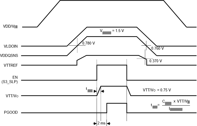
The TPS7H3301-SP provides S3 support by an EN function. The EN pin could be connected to an SLP_S3 signal in the end application. Both VTTREF and VTT/VO are on when EN = high (S0 state). VTTREF is maintained while VTT/VO is turned off and discharged via an internal discharge MOSFET when EN = low (S3 state). Please notice that the EN signal controls only the output buffer for VTT/VO and therefore, while in S3 state, VDDQSNS is present in order to maintain data in volatile memory. As a result, when EN is set high to exit the S3 state, it is desired to bring VO/VTT into regulation as fast as possible. This causes an output current controlled by the current limit of the device and the output capacitors.
When EN = low and the VDDQSNS voltage is less than 0.78 V, TPS7H3301-SP enters pseudo-S5 state. Both VTT/VO and VTTREF outputs are turned off and discharged to GND through internal MOSFETs when pseudo-S5 support is engaged (S4/S5 state). Figure 16 shows a typical startup and shutdown timing diagram for an application that uses S3 and pseudo-S5 support.
 Figure 16. Typical Timing Diagram for S3 and Pseudo-S5 Support