JAJSM19B May 2021 – December 2022 TPS7H4002-SP
PRODUCTION DATA
- 1 特長
- 2 アプリケーション
- 3 概要
- 4 Revision History
- 5 Pin Configuration and Functions
- 6 Specifications
-
7 Detailed Description
- 7.1 Overview
- 7.2 Functional Block Diagram
- 7.3
Feature Description
- 7.3.1 VIN and Power VIN Pins (VIN and PVIN)
- 7.3.2 Voltage Reference
- 7.3.3 Adjusting the Output Voltage
- 7.3.4 Safe Start-Up Into Prebiased Outputs
- 7.3.5 Error Amplifier
- 7.3.6 Slope Compensation
- 7.3.7 Enable and Adjust UVLO
- 7.3.8 Adjustable Switching Frequency and Synchronization (SYNC)
- 7.3.9 Slow Start (SS/TR)
- 7.3.10 Power Good (PWRGD)
- 7.3.11 Sequencing (SS/TR)
- 7.3.12 Output Overvoltage Protection (OVP)
- 7.3.13 Overcurrent Protection
- 7.3.14 Thermal Shutdown
- 7.3.15 Turn-On Behavior
- 7.3.16 Small Signal Model for Frequency Compensation
- 7.4 Device Functional Modes
-
8 Application and Implementation
- 8.1 Application Information
- 8.2
Typical Application
- 8.2.1 Design Requirements
- 8.2.2
Detailed Design Procedure
- 8.2.2.1 Operating Frequency
- 8.2.2.2 Output Inductor Selection
- 8.2.2.3 Output Capacitor Selection
- 8.2.2.4 Output Schottky Diode
- 8.2.2.5 Slow Start Capacitor Selection
- 8.2.2.6 Undervoltage Lockout (UVLO) Set Point
- 8.2.2.7 Output Voltage Feedback Resistor Selection
- 8.2.2.8 Compensation Component Selection
- 8.2.3 Parallel Operation
- 8.2.4 Application Curve
- 9 Power Supply Recommendations
- 10Layout
- 11Device and Documentation Support
- 12Mechanical, Packaging, and Orderable Information
パッケージ・オプション
メカニカル・データ(パッケージ|ピン)
- HKH|20
- KGD|0
サーマルパッド・メカニカル・データ
発注情報
5 Pin Configuration and Functions
Figure 5-1 HKH
Package
20-Pin CFP
Bottom View
20-Pin CFP
Bottom View
Table 5-1 Pin Functions
| PIN | I/O | DESCRIPTION | |
|---|---|---|---|
| NO. | NAME | ||
| 1 | GND | — | Return for control circuitry.(1) |
| 2 | EN | I | EN pin is internally pulled up allowing for the pin to be floated to enable the device. Adjust the input undervoltage lockout (UVLO) with two resistors. |
| 3 | RT | I/O | In internal oscillation mode, a resistor is connected between the RT pin and GND to set the switching frequency. Leaving this pin floating sets the internal switching frequency to 500 kHz. |
| 4 | SYNC | I/O | Optional 100-kHz to 1-MHz external system clock input. |
| 5 | VIN | I | Input power for the control circuitry of the switching regulator. |
| 6 | PVIN | I | Input power for the output stage of the switching regulator. |
| 7 | |||
| 8 | PGND | — | Return for low-side power MOSFET. |
| 9 | |||
| 10 | |||
| 11 | PH | O | Switch phase node. |
| 12 | |||
| 13 | |||
| 14 | |||
| 15 | |||
| 16 | REFCAP | O | Required 470-nF external capacitor for internal reference. |
| 17 | VSENSE | I | Inverting input of the gm error amplifier. |
| 18 | COMP | I/O | Error amplifier output and input to the output switch current comparator. Connect frequency compensation to this pin. |
| 19 | SS/TR | I/O | Slow-start and tracking. An external capacitor connected to this pin sets the internal voltage reference rise time. The voltage on this pin overrides the internal reference. It can be used for tracking and sequencing. |
| 20 | PWRGD | O | Power Good fault pin. Asserts low if output voltage is low due to thermal shutdown, dropout, overvoltage, or EN shutdown, or during slow start. |
(1) GND (pin 1, analog ground) must be connected to PGND external
to the package. Thermal pad must be connected to a heat dissipating layer.
Thermal pad is internally connected to the seal ring and GND.
Table 5-2 Bare Die Information
| DIE THICKNESS | BACKSIDE FINISH | BACKSIDE POTENTIAL | BOND PAD METALLIZATION COMPOSITION | BOND PAD THICKNESS |
|---|---|---|---|---|
| 15 mils | Silicon with backgrind | Ground | ALCU | 1050 nm |
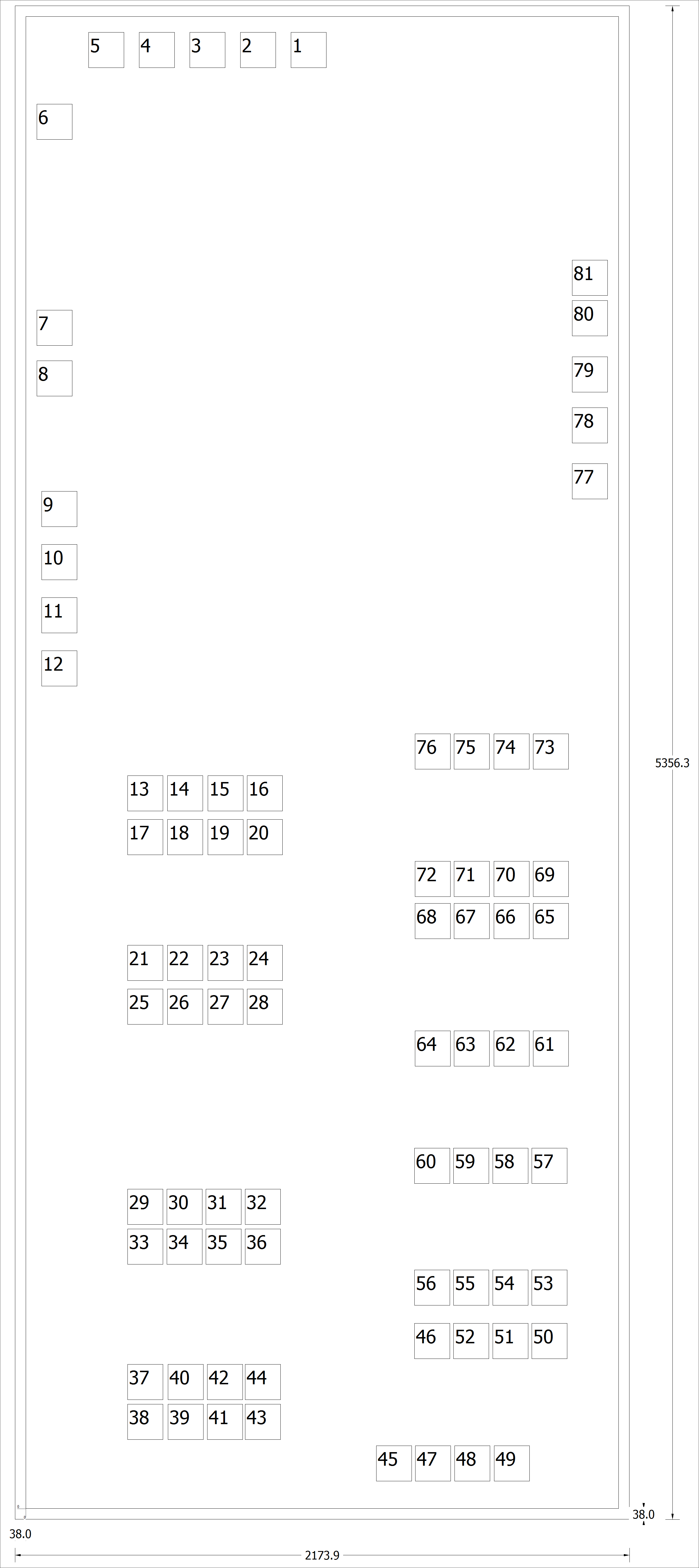
Table 5-3 Bond Pad Coordinates in
Microns
| DESCRIPTION | PAD NUMBER | X MIN | Y MIN | X MAX | Y MAX |
|---|---|---|---|---|---|
| AVSS | 1 | 938.16 | 5098.41 | 1064.16 | 5224.41 |
| AVSS | 2 | 759.06 | 5098.41 | 885.06 | 5224.41 |
| N/C | 3 | 579.96 | 5098.41 | 705.96 | 5224.41 |
| AVSS | 4 | 400.86 | 5098.41 | 526.86 | 5224.41 |
| AVSS | 5 | 221.76 | 5098.41 | 347.76 | 5224.41 |
| EN | 6 | 38.7 | 4843.98 | 164.7 | 4969.98 |
| RT | 7 | 38.7 | 4115.43 | 164.7 | 4241.43 |
| SYNC | 8 | 38.7 | 3936.33 | 164.7 | 4062.33 |
| VIN | 9 | 55.89 | 3473.865 | 181.89 | 3599.865 |
| VIN | 10 | 55.89 | 3285.765 | 181.89 | 3411.765 |
| VIN | 11 | 55.89 | 3097.665 | 181.89 | 3223.665 |
| VIN | 12 | 55.89 | 2909.565 | 181.89 | 3035.565 |
| PVIN | 13 | 360.045 | 2468.025 | 486.045 | 2594.025 |
| PVIN | 14 | 500.805 | 2468.025 | 626.805 | 2594.025 |
| PVIN | 15 | 643.905 | 2468.025 | 769.905 | 2594.025 |
| PVIN | 16 | 782.505 | 2468.025 | 908.505 | 2594.025 |
| PVIN | 17 | 360.045 | 2312.595 | 486.045 | 2438.595 |
| PVIN | 18 | 500.805 | 2312.595 | 626.805 | 2438.595 |
| PVIN | 19 | 643.905 | 2312.595 | 769.905 | 2438.595 |
| PVIN | 20 | 782.505 | 2312.595 | 908.505 | 2438.595 |
| PVIN | 21 | 360.045 | 1868.265 | 486.045 | 1994.265 |
| PVIN | 22 | 500.805 | 1868.265 | 626.805 | 1994.265 |
| PVIN | 23 | 643.905 | 1868.265 | 769.905 | 1994.265 |
| PVIN | 24 | 782.505 | 1868.265 | 908.505 | 1994.265 |
| PVIN | 25 | 360.045 | 1712.835 | 486.045 | 1838.835 |
| PVIN | 26 | 500.805 | 1712.835 | 626.805 | 1838.835 |
| PVIN | 27 | 643.905 | 1712.835 | 769.905 | 1838.835 |
| PVIN | 28 | 782.505 | 1712.835 | 908.505 | 1838.835 |
| PGND | 29 | 360 | 1004.625 | 486 | 1130.625 |
| PGND | 30 | 498.6 | 1004.625 | 624.6 | 1130.625 |
| PGND | 31 | 637.2 | 1004.625 | 763.2 | 1130.625 |
| PGND | 32 | 775.8 | 1004.625 | 901.8 | 1130.625 |
| PGND | 33 | 360 | 863.955 | 486 | 989.955 |
| PGND | 34 | 498.6 | 863.955 | 624.6 | 989.955 |
| PGND | 35 | 637.2 | 863.955 | 763.2 | 989.955 |
| PGND | 36 | 775.8 | 863.955 | 901.8 | 989.955 |
| PGND | 37 | 360 | 384.525 | 486 | 510.525 |
| PGND | 38 | 360 | 243.855 | 486 | 369.855 |
| PGND | 39 | 503.1 | 243.855 | 629.1 | 369.855 |
| PGND | 40 | 503.1 | 384.525 | 629.1 | 510.525 |
| PGND | 41 | 641.7 | 243.855 | 767.7 | 369.855 |
| PGND | 42 | 641.7 | 384.525 | 767.7 | 510.525 |
| PGND | 43 | 775.8 | 243.855 | 901.8 | 369.855 |
| PGND | 44 | 775.8 | 384.525 | 901.8 | 510.525 |
| PH | 45 | 1239.66 | 97.425 | 1365.66 | 223.425 |
| PH | 46 | 1374.66 | 529.965 | 1500.66 | 655.965 |
| PH | 47 | 1378.26 | 97.425 | 1504.26 | 223.425 |
| PH | 48 | 1516.86 | 97.425 | 1642.86 | 223.425 |
| PH | 49 | 1657.26 | 97.425 | 1783.26 | 223.425 |
| PH | 50 | 1790.46 | 529.965 | 1916.46 | 655.965 |
| PH | 51 | 1651.86 | 529.965 | 1777.86 | 655.965 |
| PH | 52 | 1513.26 | 529.965 | 1639.26 | 655.965 |
| PH | 53 | 1790.46 | 718.515 | 1916.46 | 844.515 |
| PH | 54 | 1651.86 | 718.515 | 1777.86 | 844.515 |
| PH | 55 | 1513.26 | 718.515 | 1639.26 | 844.515 |
| PH | 56 | 1374.66 | 718.515 | 1500.66 | 844.515 |
| PH | 57 | 1790.46 | 1150.065 | 1916.46 | 1276.065 |
| PH | 58 | 1651.86 | 1150.065 | 1777.86 | 1276.065 |
| PH | 59 | 1513.26 | 1150.065 | 1639.26 | 1276.065 |
| PH | 60 | 1374.66 | 1150.065 | 1500.66 | 1276.065 |
| PH | 61 | 1795.365 | 1565.1 | 1921.365 | 1691.1 |
| PH | 62 | 1655.865 | 1565.1 | 1781.865 | 1691.1 |
| PH | 63 | 1515.465 | 1565.1 | 1641.465 | 1691.1 |
| PH | 64 | 1376.865 | 1565.1 | 1502.865 | 1691.1 |
| PH | 65 | 1795.365 | 2016 | 1921.365 | 2142 |
| PH | 66 | 1655.865 | 2016 | 1781.865 | 2142 |
| PH | 67 | 1515.465 | 2016 | 1641.465 | 2142 |
| PH | 68 | 1376.865 | 2016 | 1502.865 | 2142 |
| PH | 69 | 1795.365 | 2164.86 | 1921.365 | 2290.86 |
| PH | 70 | 1655.865 | 2164.86 | 1781.865 | 2290.86 |
| PH | 71 | 1515.465 | 2164.86 | 1641.465 | 2290.86 |
| PH | 72 | 1376.865 | 2164.86 | 1502.865 | 2290.86 |
| PH | 73 | 1795.365 | 2615.76 | 1921.365 | 2741.76 |
| PH | 74 | 1655.865 | 2615.76 | 1781.865 | 2741.76 |
| PH | 75 | 1515.465 | 2615.76 | 1641.465 | 2741.76 |
| PH | 76 | 1376.865 | 2615.76 | 1502.865 | 2741.76 |
| REFCAP_NU | 77 | 1933.245 | 3572.46 | 2059.245 | 3698.46 |
| VSENSE | 78 | 1933.245 | 3770.415 | 2059.245 | 3896.415 |
| COMP | 79 | 1933.245 | 3949.515 | 2059.245 | 4075.515 |
| SS | 80 | 1933.2 | 4149.135 | 2059.2 | 4275.135 |
| PWRGD | 81 | 1933.2 | 4292.325 | 2059.2 | 4418.325 |