JAJSKK6A November 2020 – December 2021 TPS7H4010-SEP
PRODUCTION DATA
- 1 特長
- 2 アプリケーション
- 3 概要
- 4 Revision History
- 5 Pin Configuration and Functions
- 6 Specifications
-
7 Detailed Description
- 7.1 Overview
- 7.2 Functional Block Diagram
- 7.3
Feature Description
- 7.3.1 Synchronous Step-Down Regulator
- 7.3.2 Auto Mode and FPWM Mode
- 7.3.3 Fixed-Frequency Peak Current-Mode Control
- 7.3.4 Adjustable Output Voltage
- 7.3.5 Enable and UVLO
- 7.3.6 Internal LDO, VCC_UVLO, and BIAS Input
- 7.3.7 Soft Start and Voltage Tracking
- 7.3.8 Adjustable Switching Frequency
- 7.3.9 Frequency Synchronization and Mode Setting
- 7.3.10 Internal Compensation and CFF
- 7.3.11 Bootstrap Capacitor and VBOOT-UVLO
- 7.3.12 Power-Good and Overvoltage Protection
- 7.3.13 Overcurrent and Short-Circuit Protection
- 7.3.14 Thermal Shutdown
- 7.4 Device Functional Modes
-
8 Application and Implementation
- 8.1 Application Information
- 8.2
Typical Application
- 8.2.1 Design Requirements
- 8.2.2
Detailed Design Procedure
- 8.2.2.1 Output Voltage Setpoint
- 8.2.2.2 Switching Frequency
- 8.2.2.3 Input Capacitors
- 8.2.2.4 Inductor Selection
- 8.2.2.5 Output Capacitor Selection
- 8.2.2.6 Feed-Forward Capacitor
- 8.2.2.7 Bootstrap Capacitors
- 8.2.2.8 VCC Capacitor
- 8.2.2.9 BIAS
- 8.2.2.10 Soft Start
- 8.2.2.11 Undervoltage Lockout Setpoint
- 8.2.2.12 PGOOD
- 8.2.3 Application Curves
- 9 Power Supply Recommendations
- 10Layout
- 11Device and Documentation Support
- 12Mechanical, Packaging, and Orderable Information
パッケージ・オプション
デバイスごとのパッケージ図は、PDF版データシートをご参照ください。
メカニカル・データ(パッケージ|ピン)
- RNP|30
- KGD|0
サーマルパッド・メカニカル・データ
- RNP|30
発注情報
7.3.12 Power-Good and Overvoltage Protection
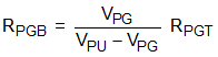
The TPS7H4010-SEP has a built-in power-good (PGOOD) flag to indicate whether the output voltage is at an appropriate level or not. The PGOOD flag can be used for start-up sequencing of multiple rails. The PGOOD pin is an open-drain output that requires a pullup resistor to an appropriate logic voltage (any voltage below 15 V). The pin can sink 5 mA of current and maintain its specified logic low level. A typical pullup resistor value is 10 kΩ to 100 kΩ. When the FB voltage is higher than VPGOOD-OV or lower than VPGOOD-UV threshold, the PGOOD internal switch is turned on, and the PGOOD pin voltage is pulled low. When the FB is within the range, the PGOOD switch is turned off, and the pin is pulled up to the voltage connected to the pullup resistor. The PGOOD function also have a deglitch timer for about 140 µs for each transition. If it is desired to pull up PGOOD pin to a voltage higher than 15 V, a resistor divider can be used to divide the voltage down.
 Figure 7-15 Divider for PGOOD Pullup Voltage
With a given pullup voltage VPU, select a desired voltage on the PGOOD pin, VPG. With a selected RPGT, the RPGB can be found by:
When the device is disabled, the output voltage is low, and the PGOOD flag indicates logic low as long as VIN > 2 V.