JAJSIR6C September 2019 – August 2021 TPS8802
PRODUCTION DATA
- 1 特長
- 2 アプリケーション
- 3 概要
- 4 Revision History
- 5 Pin Configuration and Functions
- 6 Specifications
- 7 Typical Characteristics
-
8 Detailed Description
- 8.1 Overview
- 8.2 Functional Block Diagram
- 8.3
Feature Description
- 8.3.1 System Power-up
- 8.3.2 LDO Regulators
- 8.3.3 Photo Chamber AFE
- 8.3.4 LED Driver
- 8.3.5 Carbon Monoxide Sensor AFE
- 8.3.6 Boost Converter
- 8.3.7 Interconnect Driver
- 8.3.8 Piezoelectric Horn Driver
- 8.3.9 Battery Test
- 8.3.10 AMUX
- 8.3.11 Analog Bias Block and 8 MHz Oscillator
- 8.3.12 Interrupt Signal Alerts
- 8.4 Device Functional Modes
- 8.5 Programming
- 8.6
Register Maps
- 8.6.1 REVID Register (Offset = 0h) [reset = 0h]
- 8.6.2 STATUS1 Register (Offset = 1h) [reset = 0h]
- 8.6.3 STATUS2 Register (Offset = 2h) [reset = 0h]
- 8.6.4 MASK Register (Offset = 3h) [reset = 0h]
- 8.6.5 CONFIG1 Register (Offset = 4h) [reset = 20h]
- 8.6.6 CONFIG2 Register (Offset = 5h) [reset = 2h]
- 8.6.7 ENABLE1 Register (Offset = 6h) [reset = 10h]
- 8.6.8 ENABLE2 Register (Offset = 7h) [reset = 0h]
- 8.6.9 CONTROL Register (Offset = 8h) [reset = 0h]
- 8.6.10 SLPTMR1 Register (Offset = 9h) [reset = 0h]
- 8.6.11 SLPTMR2 Register (Offset = Ah) [reset = 0h]
- 8.6.12 GPIO_AMUX Register (Offset = Bh) [reset = 0h]
- 8.6.13 CO_BATTEST Register (Offset = Ch) [reset = 0h]
- 8.6.14 CO Register (Offset = Dh) [reset = 0h]
- 8.6.15 VBOOST Register (Offset = Eh) [reset = F2h]
- 8.6.16 LEDLDO Register (Offset = Fh) [reset = 0h]
- 8.6.17 PH_CTRL Register (Offset = 10h) [reset = 0h]
- 8.6.18 LED_DAC_A Register (Offset = 11h) [reset = 0h]
- 8.6.19 LED_DAC_B Register (Offset = 12h) [reset = 0h]
- 9 Application and Implementation
- 10Power Supply Recommendations
- 11Layout
- 12Device and Documentation Support
- 13Mechanical, Packaging, and Orderable Information
パッケージ・オプション
メカニカル・データ(パッケージ|ピン)
- DCP|38
サーマルパッド・メカニカル・データ
- DCP|38
発注情報
8.3.7 Interconnect Driver
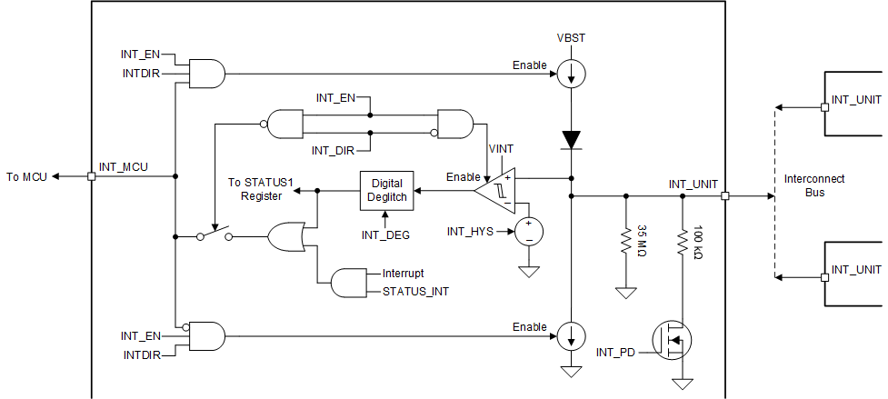
 Figure 8-8 Interconnect Driver and Receiver
In mains-wired smoke alarm systems, the alarms can alert each other of smoke conditions with a wired interconnect bus. The TPS8802 has a driver and comparator to interface with the interconnect bus. The driver pulls the bus high when smoke is detected and low when smoke is cleared. The driver is current limited to handle short circuit conditions, and has a diode on the high side driver to prevent the bus from driving VBST. The hysteretic comparator senses when the bus is pulled high, filters the signal with a digital deglitch, and outputs the result to the INT_MCU pin and STATUS1 register. The comparator output is synchronized with the 32 kHz clock. The hysteresis has two settings and the deglitch is programmable from 0 ms to 20 ms. A 35-MΩ resistor prevents the INT_UNIT pin from floating, and a switchable 100-kΩ resistor pulls down the bus to prevent leakage from causing a false alarm. When the comparator outputs a high signal through the deglitch filter, the INT_UNIT register bit is latched high in the STATUS1 register.
The INT_MCU pin has the additional function to output status interrupt signals. The STATUS_INT bit in the MASK register enables interrupt signals to output through the INT_MCU pin. When the interconnect driver is enabled, the interrupt signal output is disconnected to allow the microcontroller to drive the INT_MCU pin.