JAJSKS4A August 2021 – December 2021 TPS92519-Q1
PRODUCTION DATA
- 1 特長
- 2 アプリケーション
- 3 概要
- 4 Revision History
- 5 Pin Configuration and Functions
- 6 Specifications
-
7 Detailed Description
- 7.1 Overview
- 7.2 Functional Block Diagram
- 7.3
Feature Description
- 7.3.1 Buck Converter Switching Operation
- 7.3.2 Switching Frequency and Adaptive On-Time Control
- 7.3.3 Minimum On-Time, Off-Time, and Inductor Ripple
- 7.3.4 Enable
- 7.3.5 LED Current Regulation and Error Amplifier
- 7.3.6 Start-up Sequence
- 7.3.7 Analog Dimming and Forced Continuous Conduction Mode
- 7.3.8 External PWM Dimming and Input Undervoltage Lockout (UVLO)
- 7.3.9 Shunt FET Dimming or Matrix Beam Application
- 7.3.10 Bias Supply
- 7.3.11 Bootstrap Supply
- 7.3.12 Faults and Diagnostics
- 7.3.13 Output Short Circuit Fault
- 7.3.14 Output Open Circuit Fault
- 7.3.15 Parallel Operation
- 7.4 Device Functional Modes
-
8 Application and Implementation
- 8.1
Application Information
- 8.1.1 Duty Cycle Consideration
- 8.1.2 Switching Frequency Selection
- 8.1.3 LED Current Set Point
- 8.1.4 Inductor Selection
- 8.1.5 Output Capacitor Selection
- 8.1.6 Input Capacitor Selection
- 8.1.7 Bootstrap Capacitor Selection
- 8.1.8 Compensation Capacitor Selection
- 8.1.9 Input Undervoltage Protection
- 8.1.10 CSN Protection Diode
- 8.2
Typical Application
- 8.2.1 Design Requirements
- 8.2.2
Detailed Design Procedure
- 8.2.2.1 Calculating Duty Cycle
- 8.2.2.2 Calculating Minimum On-Time and Off-Time
- 8.2.2.3 Minimum Switching Frequency
- 8.2.2.4 LED Current Set Point
- 8.2.2.5 Inductor Selection
- 8.2.2.6 Output Capacitor Selection
- 8.2.2.7 Bootstrap Capacitor Selection
- 8.2.2.8 Compensation Capacitor Selection
- 8.2.2.9 PWM Dimming and Input Voltage Protection
- 8.2.3 Application Curves
- 8.1
Application Information
- 9 Power Supply Recommendations
- 10Layout
- 11Device and Documentation Support
- 12Mechanical, Packaging, and Orderable Information
パッケージ・オプション
メカニカル・データ(パッケージ|ピン)
- DAP|32
サーマルパッド・メカニカル・データ
- DAP|32
発注情報
7.3.14 Output Open Circuit Fault
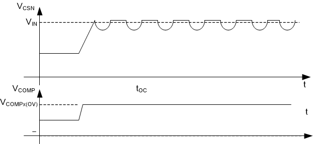
An LED open circuit fault ultimately causes the output voltage to increase and settle close to the input voltage. When this occurs, the TPS92519-Q1 switching operation is then controlled by the fixed on-time and minimum off-time resulting in a duty cycle close to 100%. Under this condition, COMP voltage exceeds VCOMPx(OV) threshold forcing FLTx flag low.
The dynamic behavior of the device and buck converter is influenced by the input voltage, VIN, and the output capacitor, COUT, value. The device response to open circuit can be categorized into the following three distinct cases.
Case 1: For a Buck converter design with a small output capacitor, the switching operation in open load condition excites the inductor and the output capacitor resonance, forcing the output voltage to oscillate. The frequency and amplitude of the oscillation are based on the resonant frequency and Q-factor of the tank.
 Figure 7-9 Open Circuit Condition With Output Voltage
Oscillation
Figure 7-9 Open Circuit Condition With Output Voltage
OscillationCase 2: For a buck converter design with larger output capacitor, the inductor Q-factor and resonant frequency are much lower than the switching frequency. In this case, output voltage rises to input voltage and the converter continues to switch with minimum off-time.
 Figure 7-10 Open Circuit Condition With Minimum Off-time
Operation