JAJSJM2B July 2022 – April 2024 TPS929240-Q1
PRODUCTION DATA
- 1
- 1 特長
- 2 アプリケーション
- 3 概要
- 4 Pin Configuration and Functions
- 5 Specifications
-
6 Detailed Description
- 6.1 Overview
- 6.2 Functional Block Diagram
- 6.3
Feature Description
- 6.3.1 Device Bias and Power
- 6.3.2 Constant Current Output
- 6.3.3 PWM Dimming
- 6.3.4 FAIL-SAFE State Operation
- 6.3.5 On-Chip, 8-Bit, Analog-to-Digital Converter (ADC)
- 6.3.6
Diagnostic and Protection in NORMAL State
- 6.3.6.1 VBAT Undervoltage Lockout Diagnostics in NORMAL state
- 6.3.6.2 Low-Supply Warning Diagnostics in NORMAL State
- 6.3.6.3 Supply Undervoltage Diagnostics in NORMAL State
- 6.3.6.4 Reference Diagnostics in NORMAL state
- 6.3.6.5 Pre-Thermal Warning in NORMAL state
- 6.3.6.6 Overtemperature Protection in NORMAL state
- 6.3.6.7 Overtemperature Shutdown in NORMAL state
- 6.3.6.8 LED Open-Circuit Diagnostics in NORMAL state
- 6.3.6.9 LED Short-Circuit Diagnostics in NORMAL state
- 6.3.6.10 Single-LED Short-Circuit Detection in NORMAL state
- 6.3.6.11 EEPROM CRC Error in NORMAL state
- 6.3.6.12 Communication Loss Diagnostic in NORMAL State
- 6.3.6.13 Fault Masking in NORMAL state
- 53
- 6.3.7
Diagnostic and Protection in FAIL-SAFE states
- 6.3.7.1 Supply Undervoltage Lockout Diagnostics in FAIL-SAFE states
- 6.3.7.2 Low-Supply Warning Diagnostics in FAIL-SAFE states
- 6.3.7.3 Supply Undervoltage Diagnostics in FAIL-SAFE State
- 6.3.7.4 Reference Diagnostics in FAIL-SAFE states
- 6.3.7.5 Pre-Thermal Warning in FAIL-SAFE state
- 6.3.7.6 Overtemperature Protection in FAIL-SAFE state
- 6.3.7.7 Overtemperature Shutdown in FAIL-SAFE state
- 6.3.7.8 LED Open-Circuit Diagnostics in FAIL-SAFE state
- 6.3.7.9 LED Short-Circuit Diagnostics in FAIL-SAFE state
- 6.3.7.10 Single-LED Short-Circuit Detection in FAIL-SAFE state
- 6.3.7.11 EEPROM CRC Error in FAIL-SAFE State
- 6.3.7.12 Fault Masking in FAIL-SAFE state
- Diagnostics Table in FAIL-SAFE State
- 6.3.8 OFAF Setup In FAIL-SAFE state
- 6.3.9 ERR Output
- 6.4 Device Functional Modes
- 6.5 Programming
- 6.6 Register Maps
- 7 Application and Implementation
- 8 Device and Documentation Support
- 9 Revision History
- 10Mechanical, Packaging, and Orderable Information
パッケージ・オプション
デバイスごとのパッケージ図は、PDF版データシートをご参照ください。
メカニカル・データ(パッケージ|ピン)
- DCP|38
サーマルパッド・メカニカル・データ
- DCP|38
発注情報
6.3.7.8 LED Open-Circuit Diagnostics in FAIL-SAFE state
The TPS929240-Q1 integrates LED open-circuit diagnostics to allow users to monitor LED status real time in FAIL-SAFE state. The device monitors voltage difference between SUPPLY and OUTXn to judge if there is any open-circuit failure. The SUPPLY voltage is also monitored in parallel with programmable threshold to determine if supply voltage is high enough for open-circuit diagnostics.
The open-circuit monitor is only effective during PWM-ON state with programmable minimal pulse width greater than t(BLANK) + t(OPEN_deg). The t(BLANK) is programmed by register BLANK. If PWM on-time is less than t(BLANK) + t(OPEN_deg), the device does not report any open-circuit fault. When the device supply voltage V(SUPPLY) is below the threshold V(LOWSUPTH) set by register LOWSUPTH, the LED open-circuit fault is not detected nor reported.
When the voltage difference V(SUPPLY) – V(OUTXn) is below threshold V(OPEN_th_rising) with duration longer than t(BLANK) + t(OPEN_deg), and the device supply voltage V(SUPPLY) is above the threshold V(LOWSUPTH), the TPS929240-Q1 pulls the ERR pin down with constant current sink to report fault and set flag registers including FLAG_OPENOUTXn, FLAG_OUT and FLAG_ERR to 1. In FAIL-SAFE state, the TPS929240-Q1 shuts down the normal current regulation and PWM dutycycle for the error output, then the device sources a current I(RETRY) to faulty output every t(SLS_Retry), 10 ms for retrying. I(RETRY) is programed by IRETRY register. The current I(RETRY) can be calculated with the below equation. When the voltage difference V(SUPPLY) – V(OUTXn) of error output rises above threshold V(OPEN_th_rising) with duration longer than t(BLANK) + t(OPEN_deg), or the supply voltage V(SUPPLY) is above the threshold V(LOWSUPTH), the device automatically resumes the normal current and PWM duty cycle setup and releases the ERR pin.
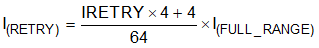
where
- IRETRY is programmable from 0 to 15.
- Use Equation 1 to calculate I(FULL_RANGE).
The fault is latched in flag registers. When the open-circuit failure is removed, the master controller must write 1 to CLRFAULT to clear FLAG_OPENOUTXn, FLAG_OUT and FLAG_ERR. The CLRFAULT bit automatically returns to 0.