JAJSPC8C December 2022 – February 2024 TPSM33615 , TPSM33625
PRODUCTION DATA
- 1
- 1 特長
- 2 アプリケーション
- 3 概要
- 4 Device Comparison Table
- 5 Pin Configuration and Functions
- 6 Specifications
-
7 Detailed Description
- 7.1 Overview
- 7.2 Functional Block Diagram
- 7.3
Feature Description
- 7.3.1 Input Voltage Range
- 7.3.2 Output Voltage Selection
- 7.3.3 Input Capacitors
- 7.3.4 Output Capacitors
- 7.3.5 Enable, Start-Up, and Shutdown
- 7.3.6 External CLK SYNC (with MODE/SYNC)
- 7.3.7 Switching Frequency (RT)
- 7.3.8 Power-Good Output Operation
- 7.3.9 Internal LDO, VCC and VOUT/FB Input
- 7.3.10 Bootstrap Voltage and VBOOT-UVLO (BOOT Terminal)
- 7.3.11 Spread Spectrum
- 7.3.12 Soft Start and Recovery from Dropout
- 7.3.13 Overcurrent Protection (Hiccup Mode)
- 7.3.14 Thermal Shutdown
- 7.4 Device Functional Modes
-
8 Application and Implementation
- 8.1 Application Information
- 8.2
Typical Application
- 8.2.1 Design Requirements
- 8.2.2
Detailed Design Procedure
- 8.2.2.1 Custom Design With WEBENCH® Tools
- 8.2.2.2 Choosing the Switching Frequency
- 8.2.2.3 Setting the Output Voltage
- 8.2.2.4 Input Capacitor Selection
- 8.2.2.5 Output Capacitor Selection
- 8.2.2.6 VCC
- 8.2.2.7 CFF Selection
- 8.2.2.8 Power Good Signal
- 8.2.2.9 Maximum Ambient Temperature
- 8.2.2.10 Other Connections
- 8.2.3 Application Curves
- 8.3 Best Design Practices
- 8.4 Power Supply Recommendations
- 8.5 Layout
- 9 Device and Documentation Support
- 10Revision History
- 11Mechanical, Packaging, and Orderable Information
7.4.3.2.1 Diode Emulation
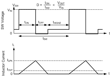
Diode emulation prevents reverse current through the inductor which potentially requires a lower frequency needed to regulate given a fixed peak inductor current. Diode emulation also limits ripple current as frequency is reduced. With a fixed peak current, as output current is reduced to zero, frequency must be reduced to near zero to maintain regulation.

The TPSM336x5 has a minimum peak inductor current setting (see IPEAKMIN in Section 6.5) while in auto mode. After current is reduced to a low value with fixed input voltage, on time is constant. Regulation is then achieved by adjusting frequency. This mode of operation is called PFM mode regulation.