SLWS213A January 2010 – November 2015 TRF370417
PRODUCTION DATA.
- 1 Features
- 2 Applications
- 3 Description
- 4 Revision History
- 5 Pin Configuration and Functions
- 6 Specifications
- 7 Detailed Description
- 8 Application and Implementation
- 9 Power Supply Recommendations
- 10Layout
- 11Device and Documentation Support
- 12Mechanical, Packaging, and Orderable Information
パッケージ・オプション
メカニカル・データ(パッケージ|ピン)
- RGE|24
サーマルパッド・メカニカル・データ
- RGE|24
発注情報
8 Application and Implementation
NOTE
Information in the following applications sections is not part of the TI component specification, and TI does not warrant its accuracy or completeness. TI’s customers are responsible for determining suitability of components for their purposes. Customers should validate and test their design implementation to confirm system functionality.
8.1 Application Information
8.1.1 Basic Connections
- See Figure 39 for proper connection of the TRF3704 modulator.
- Connect a single power supply (4.5 V–5.5 V) to pins 18 and 24. These pins should be decoupled as shown on pins 4, 5, 6, and 7.
- Connect pins 2, 5, 8, 11, 12, 14, 17, 19, 20, and 23 to GND.
- Connect a single-ended LO source of desired frequency to LOP (amplitude between –5 dBm and 12 dBm). This should be ac-coupled through a 100-pF capacitor.
- Terminate the ac-coupled LON with 50 Ω to GND.
- Connect a baseband signal to pins 21 = I, 22 = I, 10 = Q, and 9 = Q.
- The differential baseband inputs should be set to the proper common-mode voltage of 1.7 V.
- RF_OUT, pin 16, can be fed to a spectrum analyzer set to the desired frequency, LO ± baseband signal. This pin should also be ac-coupled through a 100-pF capacitor.
- All NC pins can be left floating.
8.1.1.1 ESD Sensitivity
RF devices may be extremely sensitive to electrostatic discharge (ESD). To prevent damage from ESD, devices should be stored and handled in a way that prevents the build-up of electrostatic voltages that exceed the rated level. Rated ESD levels should also not be exceeded while the device is installed on a printed circuit board (PCB). Follow these guidelines for optimal ESD protection:
- Low ESD performance is not uncommon in RF ICs; see the Absolute Maximum Ratings table. Therefore, customers’ ESD precautions should be consistent with these ratings.
- The device should be robust once assembled onto the PCB unless external inputs (connectors, etc.) directly connect the device pins to off-board circuits.
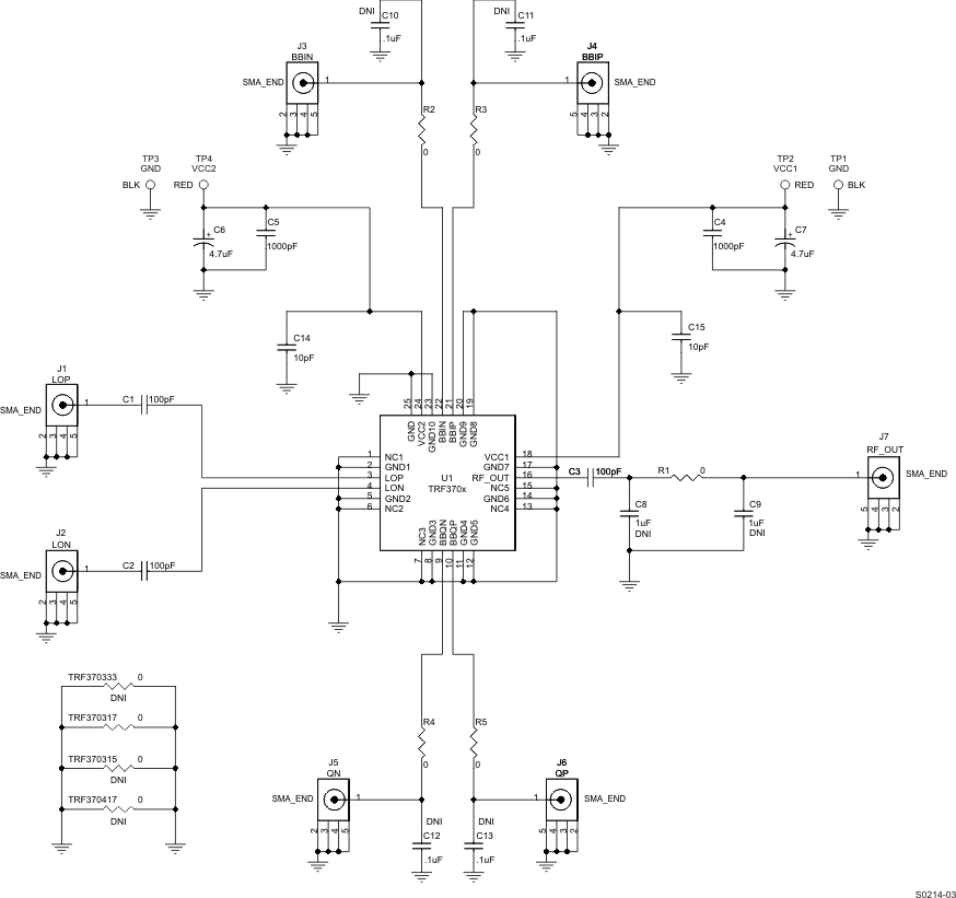
NOTE:
DNI = Do not install.8.1.2 GSM Applications
The TRF370417 is suited for GSM and multicarrier GSM applications because of its high linearity and low noise level over the entire recommended operating range. It also has excellent EVM performance, which makes it ideal for the stringent GSM/EDGE applications.
8.1.3 WCDMA Applications
The TRF370417 is also optimized for WCDMA applications where both adjacent-channel power ratio (ACPR) and noise density are critically important. Using Texas instruments’ DAC568X series of high-performance digital-to-analog converters as depicted in Figure 39, excellent ACPR levels were measured with one-, two-, and four-WCDMA carriers. See Electrical Characteristics, fLO = 1960 MHz and fLO = 2140 MHz for exact ACPR values.
8.2 Typical Application
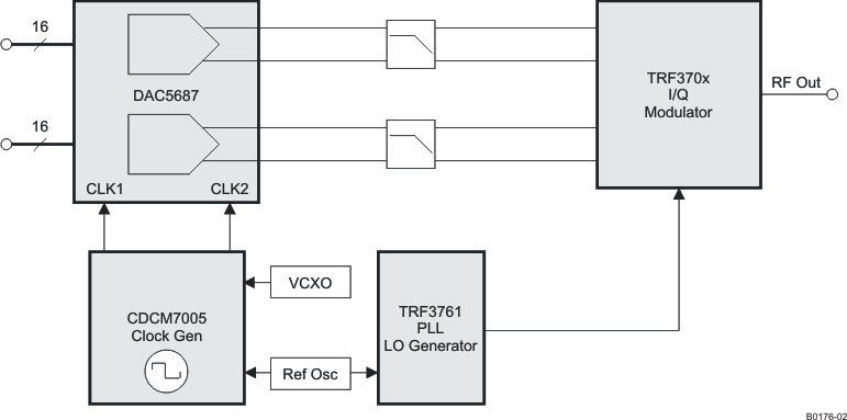 Figure 40. Typical Transmit Setup Block Diagram
8.2.1 Design Requirements
Table 1 lists the requirements and limitations for pin termination.
Table 1. Pin Termination Requirements and Limitations
| NAME | PIN NO. | DESCRIPTION |
|---|---|---|
| BBQM | 9 | Baseband in-quadrature input: negative terminal. Optimal linearity is obtained if VCM is 1.7-V. Normally terminated in 50 Ω |
| BBQP | 10 | Baseband in-quadrature input: positive terminal. Optimal linearity is obtained if VCM is 1.7-V. Normally terminated in 50 Ω |
| BBIP | 21 | Baseband in-phase input: positive terminal. Optimal linearity is obtained if VCM is 1.7-V. Normally terminated in 50 Ω |
| BBIM | 22 | Baseband in-phase input: negative terminal. Optimal linearity is obtained if VCM is 1.7-V. Normally terminated in 50 Ω |
| LOP | 3 | Local oscillator input: positive terminal. This is preferred port when driving single ended. Normally AC coupled and terminated in 50 Ω |
| LOM | 4 | Local oscillator input: negative terminal. When driving LO single-ended, normally AC coupled and terminated in 50 Ω. |
| RFOUT | 16 | RF output. Normally AC coupled. Recommend to terminate with broadband 50- Ω load. |
| VCC | 18, 24 | 5.0-V power supply. Can be tied together and sourced from a single clean supply. Each pin should be properly RF bypassed. |
8.2.2 Detailed Design Procedure
Table 2. Bill of Materials for TRF370x EVM
| ITEM NUMBER | QUANTITY | REFERENCE DESIGNATOR | VALUE | PCB FOOTPRINT | MFR. NAME | MFT. PART NUMBER | NOTE |
|---|---|---|---|---|---|---|---|
| 1 | 3 | C1, C2, C3 | 100 pF | 0402 | PANASONIC | ECJ-0EC1H101J | |
| 2 | 2 | C4, C5 | 1000 pF | 0402 | PANASONIC | ECJ-0VC1H102J | |
| 3 | 2 | C6, C7 | 4.7 μF | TANT_A | KERMET | T491A475K016AS | |
| 4 | 0 | C8, C9 | 1 μF | 0402 | PANASONIC | ECJ-0EC1H010C_DNI | DNI |
| 5 | 0 | C10, C11, C12, C13 | 0.1 μF | 0402 | PANASONIC | ECJ-0EB1A104K_DNI | DNI |
| 6 | 2 | C14, C15 | 10 pF | 0402 | MURATA | GRM1555C1H100JZ01D | |
| 7 | 7 | J1, J2, J3, J4, J5, J6, J7 | LOP | SMA_SMEL_250x215 | JOHNSON COMPONENTS | 142-0711-821 | |
| 8 | 2 | R1 | 0 | 0402 | PANASONIC | ERJ-2GE0R00 | OR EQUIVALENT |
| 9 | 4 | R2, R3, R4, R5 | 0 | 0402 | PANASONIC | ERJ-2GE0R00 | OR EQUIVALENT |
| 10 | 1 | U1 | TRF370333 | QFN_24_163x163_ 0p50mm |
TI | TRF370333 | For TRF370333 EVM, TI supplied |
| TRF370317 | QFN_24_163x163_ 0p50mm |
TI | TRF370317 | For TRF370317 EVM, TI supplied | |||
| TRF370315 | QFN_24_163x163_ 0p50mm |
TI | TRF370315 | For TRF370315 EVM, TI supplied | |||
| TRF370417 | QFN_24_163x163_ 0p50mm |
TI | TRF370417 | For TRF370417 EVM, TI supplied | |||
| 11 | 2 | TP1, TP3 | BLK | TP_THVT_100_RND | KEYSTONE | 5001K | |
| 12 | 2 | TP2, TP4 | RED | TP_THVT_100_RND | KEYSTONE | 5000K |
8.2.2.1 DAC-to-Modulator Interface Network
For optimum linearity and dynamic range, the digital-to-analog converter (DAC) can interface directly with the modulator; however, the common-mode voltage of each device must be maintained. A passive interface circuit is used to transform the common-mode voltage of the DAC to the desired set-point of the modulator. The passive circuit invariably introduces some insertion loss between the two devices. In general, it is desirable to keep the insertion loss as low as possible to achieve the best dynamic range. Figure 41 shows the passive interconnect circuit for two different topologies. One topology is used when the DAC (such as the DAC568x) common-mode is larger than the modulator. The voltage Vee is nominally set to ground, but can be set to a negative voltage to reduce the insertion loss of the network. The second topology is used when the DAC (such as the DAC56x2) common-mode is smaller than the modulator. Note that this passive interconnect circuit is duplicated for each of the differential I/Q branches.
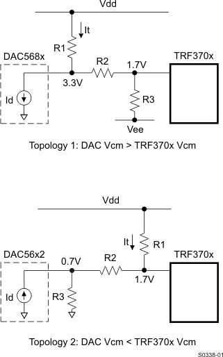 Figure 41. Passive DAC-to-Modulator Interface Network
Table 3. DAC-to-Modulator Interface Network Values
| TOPOLOGY 1 | TOPOLOGY 2 | ||
|---|---|---|---|
| WITH VEE = 0 V | WITH VEE = 5 V | ||
| DAC Vcm [V] | 3.3 | 3.3 | 0.7 |
| TRF370x Vcm [V] | 1.7 | 1.7 | 1.7 |
| Vdd [V] | 5 | 5 | 5 |
| Vee [V] | Gnd | –5 | N/A |
| R1 [Ω] | 66 | 56 | 960 |
| R2 [Ω] | 100 | 80 | 290 |
| R3 [Ω] | 108 | 336 | 52 |
| Insertion loss [dB] | 5.8 | 1.9 | 2.3 |
8.2.3 Application Curves
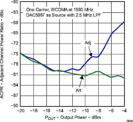 Figure 42. Adjacent Channel Power Ratio vs Output Power at 1960 MHz
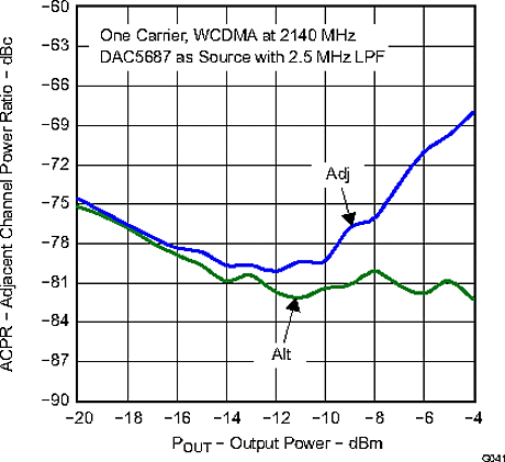 Figure 43. Adjacent Channel Power Ratio vs. Output Power at 2140 MHz