SLWS213A January 2010 – November 2015 TRF370417
PRODUCTION DATA.
- 1 Features
- 2 Applications
- 3 Description
- 4 Revision History
- 5 Pin Configuration and Functions
- 6 Specifications
- 7 Detailed Description
- 8 Application and Implementation
- 9 Power Supply Recommendations
- 10Layout
- 11Device and Documentation Support
- 12Mechanical, Packaging, and Orderable Information
パッケージ・オプション
メカニカル・データ(パッケージ|ピン)
- RGE|24
サーマルパッド・メカニカル・データ
- RGE|24
発注情報
6 Specifications
6.1 Absolute Maximum Ratings
over operating free-air temperature range (unless otherwise noted)(1)| MIN | MAX | UNIT | ||
|---|---|---|---|---|
| Supply voltage range | –0.3 | 6 | V | |
| TJ | Operating virtual junction temperature range | –40 | 150 | °C |
| TA | Operating ambient temperature range | –40 | 85 | °C |
| Tstg | Storage temperature range | –65 | 150 | °C |
(1) Stresses beyond those listed under Absolute Maximum Ratings may cause permanent damage to the device. These are stress ratings only, which do not imply functional operation of the device at these or any other conditions beyond those indicated under Recommended Operating Conditions. Exposure to absolute-maximum-rated conditions for extended periods may affect device reliability.
6.2 ESD Ratings
| VALUE | UNIT | |||
|---|---|---|---|---|
| V(ESD) | Electrostatic discharge | Human-body model (HBM), per ANSI/ESDA/JEDEC JS-001(1) | ±75 | V |
| Charged-device model (CDM), per JEDEC specification JESD22-C101(2) | ±75 | |||
(1) JEDEC document JEP155 states that 500-V HBM allows safe manufacturing with a standard ESD control process.
(2) JEDEC document JEP157 states that 250-V CDM allows safe manufacturing with a standard ESD control process.
6.3 Recommended Operating Conditions
over operating free-air temperature range (unless otherwise noted)| MIN | NOM | MAX | UNIT | ||
|---|---|---|---|---|---|
| VCC | Power-supply voltage | 4.5 | 5 | 5.5 | V |
6.4 Thermal Information
| THERMAL METRIC(1) | TRF370417 | UNIT | |
|---|---|---|---|
| RGE (VQFN) | |||
| 24 PINS | |||
| RθJA | Junction-to-ambient thermal resistance (High-K board, still air) | 29.4 | °C/W |
| RθJC(top) | Junction-to-case (top) thermal resistance | 18.6 | °C/W |
| RθJB | Junction-to-board thermal resistance | 14 | °C/W |
| ψJT | Junction-to-top characterization parameter | — | °C/W |
| ψJB | Junction-to-board characterization parameter | — | °C/W |
| RθJC(bot) | Junction-to-case (bottom) thermal resistance | — | °C/W |
(1) For more information about traditional and new thermal metrics, see the Semiconductor and IC Package Thermal Metrics application report, SPRA953.
6.5 Electrical Characteristics
over operating free-air temperature range (unless otherwise noted)| PARAMETER | TEST CONDITIONS | MIN | TYP | MAX | UNIT | ||
|---|---|---|---|---|---|---|---|
| DC Parameters | |||||||
| ICC | Total supply current (1.7 V CM) | TA = 25°C | 205 | 245 | mA | ||
| LO Input (50-Ω, Single-Ended) | |||||||
| fLO | LO frequency range | 0.05 | 6 | GHz | |||
| LO input power | –5 | 0 | 12 | dBm | |||
| LO port return loss | 15 | dB | |||||
| Baseband Inputs | |||||||
| VCM | I and Q input dc common voltage | 1.7 | |||||
| BW | 1-dB input frequency bandwidth | 1 | GHz | ||||
| ZI(single ended) | Input impedance, resistance | 5 | kΩ | ||||
| Input impedance, parallel capacitance | 3 | pF | |||||
6.6 RF Output Parameters
over recommended operating conditions, power supply = 5 V, TA = 25°C, VCM = 1.7 V, VinBB = 98 mVrms single-ended in quadrature, fBB = 50 kHz (unless otherwise noted)| PARAMETER | TEST CONDITIONS | MIN | TYP | MAX | UNIT | ||
|---|---|---|---|---|---|---|---|
| fLO = 70 MHz at 8 dBm | |||||||
| G | Voltage gain | Output rms voltage over input I (or Q) rms voltage | –8 | dB | |||
| P1dB | Output compression point | 7.3 | dBm | ||||
| IP3 | Output IP3 | fBB = 4.5, 5.5 MHz; Pout = –8 dBm per tone | 22 | dBm | |||
| IP2 | Output IP2 | fBB = 4.5, 5.5 MHz; Pout = –8 dBm per tone | 69 | dBm | |||
| Carrier feedthrough | Unadjusted | –46 | dBm | ||||
| Sideband suppression | Unadjusted; fBB = 4.5, 5.5 MHz | –27.5 | dBc | ||||
| fLO = 400 MHz at 8 dBm | |||||||
| G | Voltage gain | Output rms voltage over input I (or Q) rms voltage | –1.9 | dB | |||
| P1dB | Output compression point | 11 | dBm | ||||
| IP3 | Output IP3 | fBB = 4.5, 5.5 MHz; Pout = –8 dBm per tone | 24.5 | dBm | |||
| IP2 | Output IP2 | fBB = 4.5, 5.5 MHz; Pout = –8 dBm per tone | 68 | dBm | |||
| Carrier feedthrough | Unadjusted | –38 | dBm | ||||
| Sideband suppression | Unadjusted; fBB = 4.5, 5.5 MHz | –40 | dBc | ||||
| fLO = 945.6 MHz at 8 dBm | |||||||
| G | Voltage gain | Output rms voltage over input I (or Q) rms voltage | –2.5 | dB | |||
| P1dB | Output compression point | 11 | dBm | ||||
| IP3 | Output IP3 | fBB = 4.5, 5.5 MHz; Pout = –8 dBm per tone | 25 | dBm | |||
| IP2 | Output IP2 | fBB = 4.5, 5.5 MHz; Pout = –8 dBm per tone | 65 | dBm | |||
| Carrier feedthrough | Unadjusted | –40 | dBm | ||||
| Sideband suppression | Unadjusted; fBB = 4.5, 5.5 MHz | –42 | dBc | ||||
| Output return loss | 9 | dB | |||||
| Output noise floor | ≥13 MHz offset from fLO; Pout = –5 dBm | –161.2 | dBm/Hz | ||||
| fLO = 1800 MHz at 8 dBm | |||||||
| G | Voltage gain | Output rms voltage over input I (or Q) rms voltage | –2.5 | dB | |||
| P1dB | Output compression point | 12 | dBm | ||||
| IP3 | Output IP3 | fBB = 4.5, 5.5 MHz; Pout = –8 dBm per tone | 26 | dBm | |||
| IP2 | Output IP2 | fBB = 4.5, 5.5 MHz; Pout = –8 dBm per tone | 60 | dBm | |||
| Carrier feedthrough | Unadjusted | –40 | dBm | ||||
| Sideband suppression | Unadjusted; fBB = 4.5, 5.5 MHz | –50 | dBc | ||||
| Output return loss | 8 | dB | |||||
| Output noise floor | ≥13 MHz offset from fLO; Pout = –5 dBm | –161.5 | dBm/Hz | ||||
| fLO = 1960 MHz at 8 dBm | |||||||
| G | Voltage gain | Output rms voltage over input I (or Q) rms voltage | –2.5 | dB | |||
| P1dB | Output compression point | 12 | dBm | ||||
| IP3 | Output IP3 | fBB = 4.5, 5.5 MHz; Pout = –8 dBm per tone | 26.5 | dBm | |||
| IP2 | Output IP2 | fBB = 4.5, 5.5 MHz; Pout = –8 dBm per tone | 60 | dBm | |||
| Carrier feedthrough | Unadjusted | –38 | dBm | ||||
| Sideband suppression | Unadjusted; fBB = 4.5, 5.5 MHz | –50 | dBc | ||||
| Output return loss | 8 | dB | |||||
| Output noise floor | ≥13 MHz offset from fLO; Pout = –5 dBm | –162 | dBm/Hz | ||||
| EVM | Error vector magnitude (rms) | 1 EDGE signal, Pout = –5 dBm(1) | 0.43% | ||||
| ACPR | Adjacent-channel power ratio | 1 WCDMA signal; Pout = –8 dBm(3) | –76 | dBc | |||
| 1 WCDMA signal; Pout = –8 dBm(2) | –74 | ||||||
| 2 WCDMA signals; Pout = –11 dBm per carrier(2) | –68 | ||||||
| 4 WCDMA signals; Pout = –14 dBm per carrier(2) | –67 | ||||||
| Alternate-channel power ratio | 1 WCDMA signal; Pout = –8 dBm(3) | –80 | dBc | ||||
| 1 WCDMA signal; Pout = –8 dBm(2) | –78 | ||||||
| 2 WCDMA signals; Pout = –11 dBm per carrier(2) | –72 | ||||||
| 4 WCDMA signals; Pout = –14 dBm per carrier(2) | –69 | ||||||
| fLO = 2140 MHz at 8 dBm | |||||||
| G | Voltage gain | Output rms voltage over input I (or Q) rms voltage | –2.4 | dB | |||
| P1dB | Output compression point | 12 | dBm | ||||
| IP3 | Output IP3 | fBB = 4.5, 5.5 MHz; Pout = –8 dBm per tone | 26.5 | dBm | |||
| IP2 | Output IP2 | fBB = 4.5, 5.5 MHz; Pout = –8 dBm per tone | 66 | dBm | |||
| Carrier feedthrough | Unadjusted | –38 | dBm | ||||
| Sideband suppression | Unadjusted; fBB = 4.5, 5.5 MHz | –50 | dBc | ||||
| Output return loss | 8.5 | dB | |||||
| Output noise floor | ≥13 MHz offset from fLO ; Pout = –5 dBm | –162.3 | dBm/Hz | ||||
| ACPR | Adjacent-channel power ratio | 1 WCDMA signal; Pout = –8 dBm(3) | –76 | dBc | |||
| 1 WCDMA signal; Pout = –8 dBm(2) | –72 | ||||||
| 2 WCDMA signal; Pout = –11 dBm per carrier(2) | –67 | ||||||
| 4 WCDMA signals; Pout = –14 dBm per carrier(2) | –66 | ||||||
| Alternate-channel power ratio | 1 WCDMA signal; Pout = –8 dBm(3) | –80 | dBc | ||||
| 1 WCDMA signal; Pout = –8 dBm(2) | –78 | ||||||
| 2 WCDMA signal; Pout = –11 dBm(2) | –74 | ||||||
| 4 WCDMA signals; Pout = –14 dBm per carrier(2) | –68 | ||||||
| fLO = 2500 MHz at 8 dBm | |||||||
| G | Voltage gain | Output rms voltage over input I (or Q) rms voltage | –1.6 | dB | |||
| P1dB | Output compression point | 13 | dBm | ||||
| IP3 | Output IP3 | fBB = 4.5, 5.5 MHz; Pout = –8 dBm per tone | 29 | dBm | |||
| IP2 | Output IP2 | fBB = 4.5, 5.5 MHz; Pout = –8 dBm per tone | 65 | dBm | |||
| Carrier feedthrough | Unadjusted | –37 | dBm | ||||
| Sideband suppression | Unadjusted; fBB = 4.5, 5.5 MHz | –47 | dBc | ||||
| EVM | Error vector magnitude (rms) | WiMAX 5-MHz carrier, Pout = –8 dBm(4) | –47 | dB | |||
| WiMAX 5-MHz carrier, Pout = 0 dBm(4) | –45 | dB | |||||
| fLO = 3500 MHz at 8 dBm | |||||||
| G | Voltage gain | Output rms voltage over input I (or Q) rms voltage | 0.6 | dB | |||
| P1dB | Output compression point | 13.5 | dBm | ||||
| IP3 | Output IP3 | fBB = 4.5, 5.5 MHz | 25 | dBm | |||
| IP2 | Output IP2 | fBB = 4.5, 5.5 MHz | 65 | dBm | |||
| Carrier feedthrough | Unadjusted | –35 | dBm | ||||
| Sideband suppression | Unadjusted; fBB = 4.5, 5.5 MHz | –36 | dBc | ||||
| EVM | Error vector magnitude (rms) | WiMAX 5-MHz carrier, Pout = –8 dBm(4) | –47 | dB | |||
| WiMAX 5-MHz carrier, Pout = 0 dBm(4) | –43 | dB | |||||
| fLO = 4000 MHz at 8 dBm | |||||||
| G | Voltage gain | Output rms voltage over input I (or Q) rms voltage | 0.2 | dB | |||
| P1dB | Output compression point | 12 | dBm | ||||
| IP3 | Output IP3 | fBB = 4.5, 5.5 MHz | 22.5 | dBm | |||
| IP2 | Output IP2 | fBB = 4.5, 5.5 MHz | 60 | dBm | |||
| Carrier feedthrough | Unadjusted | –36 | dBm | ||||
| Sideband suppression | Unadjusted; fBB = 4.5, 5.5 MHz | –36 | dBc | ||||
| fLO = 5800 MHz at 4 dBm | |||||||
| G | Voltage gain | Output rms voltage over input I (or Q) rms voltage | –5.5 | dB | |||
| P1dB | Output compression point | 12.9 | dBm | ||||
| IP3 | Output IP3 | fBB = 4.5, 5.5 MHz | 25 | dBm | |||
| IP2 | Output IP2 | fBB = 4.5, 5.5 MHz | 55 | dBm | |||
| Carrier feedthrough | Unadjusted | –31 | dBm | ||||
| Sideband suppression | Unadjusted; fBB = 4.5, 5.5 MHz | –36 | dBc | ||||
| EVM | Error-vector magnitude | WiMAX 5-MHz carrier, Pout = –12 dBm(4) | –40 | dB | |||
(1) The contribution from the source of about 0.28% is not de-embedded from the measurement.
(2) Measured with DAC5687 as source generator; no external BB filters are used.
(3) Measured with DAC5687 as source generator; with 2.5 MHz LPF.
(4) Sideband suppression optimized with LO drive level; EVM contribution from instrument is not accounted for.
6.7 Typical Characteristics
VCM = 1.7 V, VinBB = 98 mVrms single-ended sine wave in quadrature, VCC = 5 V, LO power = 4 dBm (single-ended), fBB = 50 kHz (unless otherwise noted). Figure 1. Output Power vs Baseband Voltage
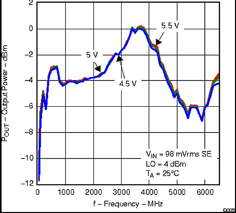 Figure 3. Output Power vs Frequency and Supply Voltage
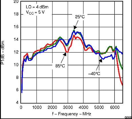 Figure 5. P1dB vs Frequency and Temperature
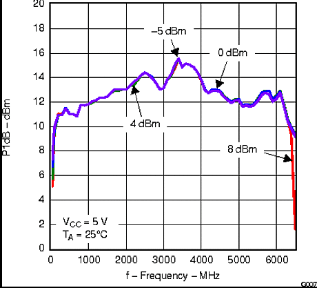 Figure 7. P1dB vs Frequency and LO Power
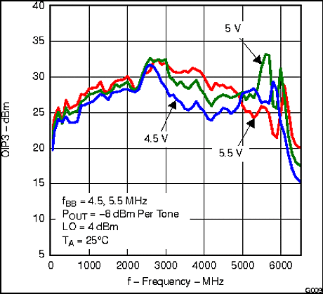 Figure 9. OIP3 vs Frequency and Supply Voltage
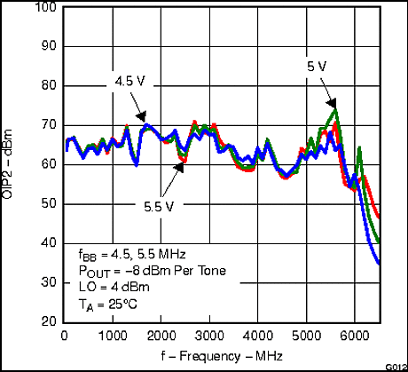 Figure 11. OIP2 vs Frequency and Supply Voltage
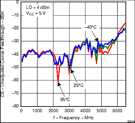 Figure 13. Unadjusted Carrier Feedthrough vs Frequency and Temperature
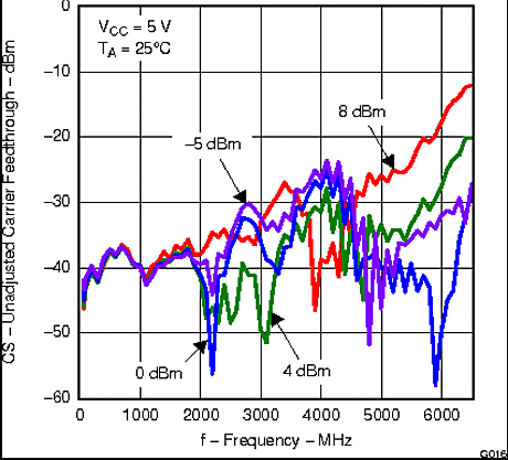 Figure 15. Unadjusted Carrier Feedthrough vs Frequency and LO Power
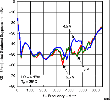 Figure 17. Unadjusted Sideband Suppression vs Frequency and Supply Voltage
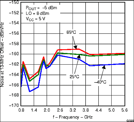 Figure 19. Noise at 13-MHz Offset (dBm/Hz) vs Frequency and Temperature
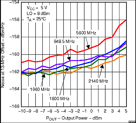 Figure 21. Noise at 13-MHz Offset (dBm/Hz) vs Output Power
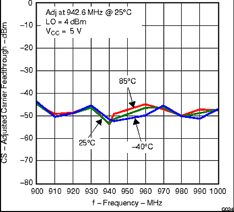 Figure 23. Adjusted Carrier Feedthrough vs Frequency and Temperature
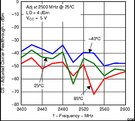 Figure 25. Adjusted Carrier Feedthrough vs Frequency and Temperature
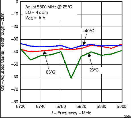 Figure 27. Adjusted Carrier Feedthrough vs Frequency and Temperature
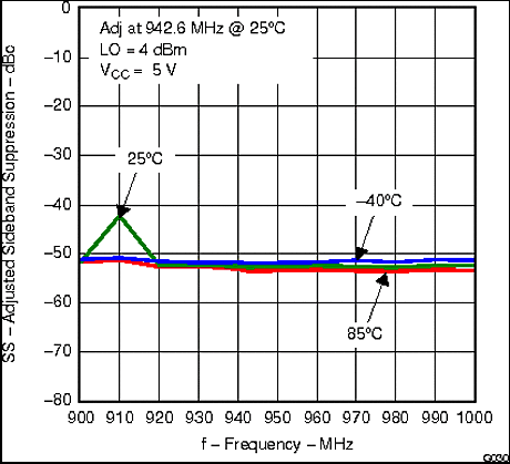 Figure 29. Adjusted Sideband Supression vs Frequency and Temperature
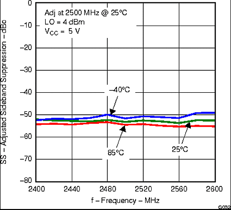 Figure 31. Adjusted Sideband Supression vs Frequency and Temperature
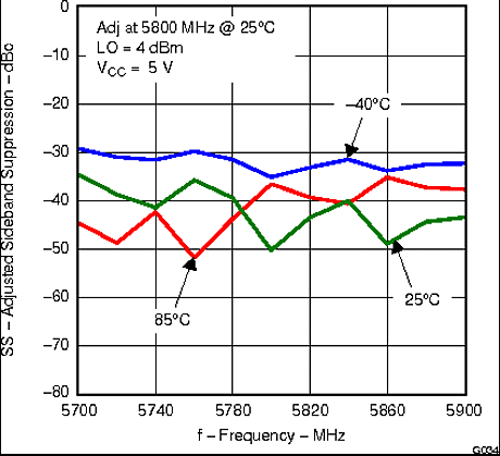 Figure 33. Adjusted Sideband Supression vs Frequency and Temperature
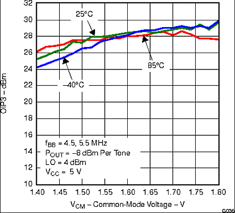 Figure 35. OIP3 vs Common-Mode Voltage at 1800 MHz
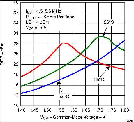 Figure 37. OIP3 vs Common-Mode Voltage at 5800 MHz
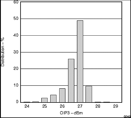 OIP3 at 1960 MHz Distribution
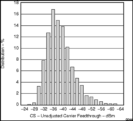 Unadjusted Carrier Feedthrough at 1960 MHz Distribution
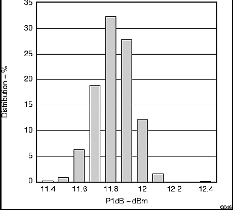 P1dB at 1800 MHz Distribution
 Figure 2. Output Power vs Frequency and Temperature
 Figure 4. Output Power vs Frequency and LO Power
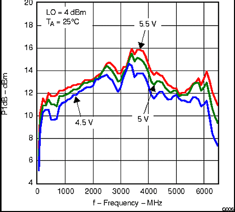 Figure 6. P1dB vs Frequency and Supply Voltage
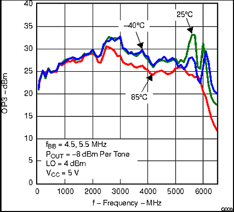 Figure 8. OIP3 vs Frequency and Temperature
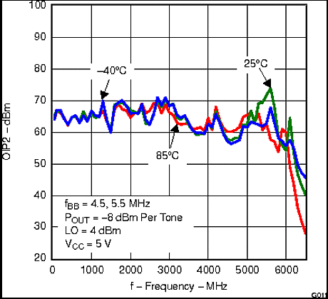 Figure 10. OIP2 vs Frequency and Temperature
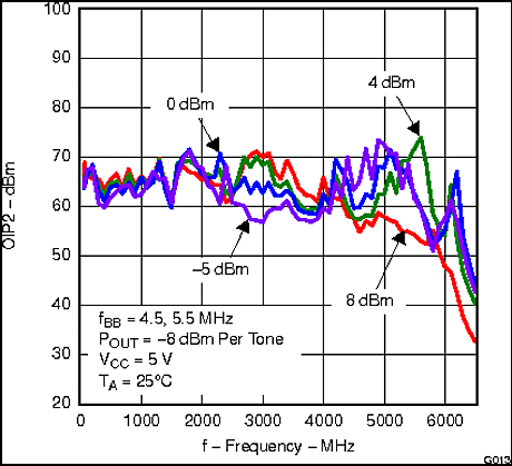 Figure 12. OIP2 vs Frequency and LO POWER
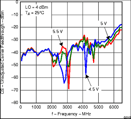 Figure 14. Unadjusted Carrier Feedthrough vs Frequency and Supply Voltage
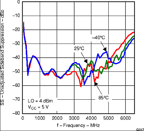 Figure 16. Unadjusted Sideband Suppression vs Frequency and Temperature
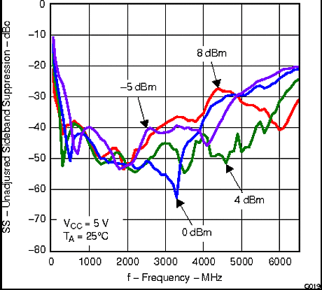 Figure 18. Unadjusted Sideband Suppression vs Frequency and LO Power
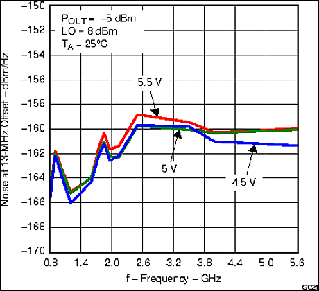 Figure 20. Noise at 13-MHz Offset (dBm/Hz) vs Frequency and Supply Voltage
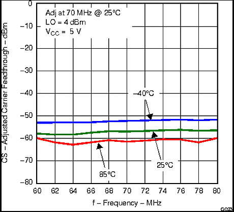 Figure 22. Adjusted Carrier Feedthrough vs Frequency and Temperature
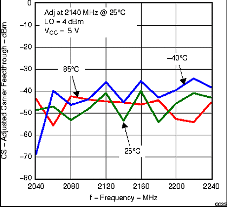 Figure 24. Adjusted Carrier Feedthrough vs Frequency and Temperature
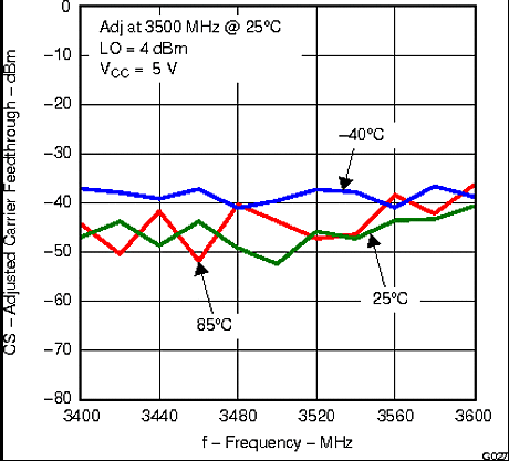 Figure 26. Adjusted Carrier Feedthrough vs Frequency and Temperature
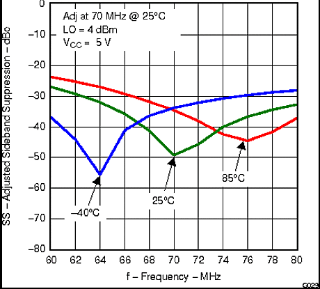 Figure 28. Adjusted Sideband Supression vs Frequency and Temperature
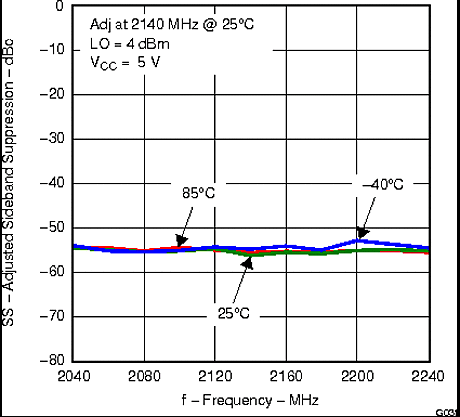 Figure 30. Adjusted Sideband Supression vs Frequency and Temperature
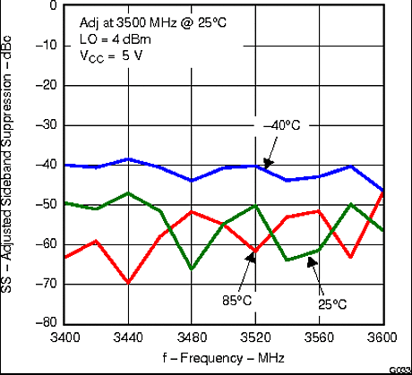 Figure 32. Adjusted Sideband Supression vs Frequency and Temperature
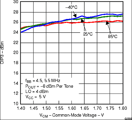 Figure 34. OIP3 vs Common-Mode Voltage at 948.5 MHz
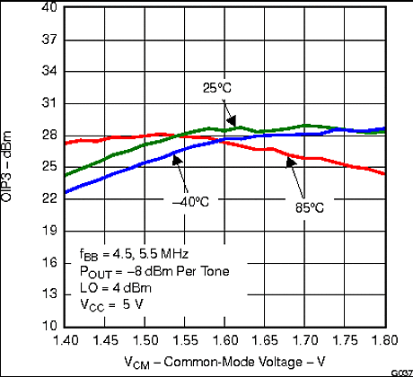 Figure 36. OIP3 vs Common-Mode Voltage at 2140 MHz
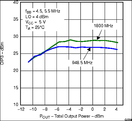 Figure 38. OIP3 vs Total Output Power
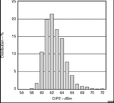 OIP2 at 1960 MHz Distribution
 Unadjusted Sideband Suppression at 1960 MHz Distribution