SCES638D October 2007 – June 2017 TXS0101
PRODUCTION DATA.
- 1 Features
- 2 Applications
- 3 Description
- 4 Revision History
- 5 Pin Configuration and Functions
-
6 Specifications
- 6.1 Absolute Maximum Ratings
- 6.2 ESD Ratings
- 6.3 Recommended Operating Conditions
- 6.4 Thermal Information
- 6.5 Electrical Characteristics
- 6.6 Timing Requirements: V CCA = 1.8 V ± 0.15 V
- 6.7 Timing Requirements VCCA = 2.5 V ± 0.2 V
- 6.8 Timing Requirements: 3.3 V ± 0.3 V
- 6.9 Switching Characteristics: VCCA = 1.8 V ± 0.15 V
- 6.10 Switching Characteristics: VCCA = 2.5 V ± 0.2 V
- 6.11 Switching Characteristics: VCCA = 3.3 V ± 0.3 V
- 6.12 Typical Characteristics
- 7 Parameter Measurement Information
- 8 Detailed Description
- 9 Application and Implementation
- 10Power Supply Recommendations
- 11Layout
- 12Device and Documentation Support
- 13Mechanical, Packaging, and Orderable Information
パッケージ・オプション
メカニカル・データ(パッケージ|ピン)
サーマルパッド・メカニカル・データ
- DCK|6
発注情報
9 Application and Implementation
NOTE
Information in the following applications sections is not part of the TI component specification, and TI does not warrant its accuracy or completeness. TI’s customers are responsible for determining suitability of components for their purposes. Customers should validate and test their design implementation to confirm system functionality.
9.1 Application Information
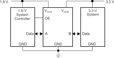
The TXS0101 can be used in level-translation applications for interfacing devices or systems operating at different interface voltages with one another. The TXS0101 is ideal for use in applications where an open-drain driver is connected to the data I/Os. The TXB0101 can also be used in applications where a push-pull driver is connected to the data I/Os, but the TXB0102 might be a better option for such push-pull applications.
9.2 Typical Application
 Figure 11. Typical Application Schematic
9.2.1 Design Requirements
For this design example, use the parameters listed in Table 1.
Table 1. Design Parameters
| DESIGN PARAMETER | EXAMPLE VALUE |
|---|---|
| Input voltage range | 1.65 to 3.6 V |
| Output voltage range | 2.3 to 5.5 V |
9.2.2 Detailed Design Procedure
To begin the design process, determine the following:
- Input voltage range
- Use the supply voltage of the device that is driving the TXS0101 device to determine the input voltage range. For a valid logic high the value must exceed the VIH of the input port. For a valid logic low the value must be less than the VIL of the input port.
- Output voltage range
- Use the supply voltage of the device that the TXS0101 device is driving to determine the output voltage range.
- The TXS0101 device has 10 kΩ internal pullup resistors. External pullup resistors can be added to reduce the total RC of a signal trace if necessary.
- An external pull down resistor decreases the output VOH and VOL. Use Equation 1 to calculate the VOH as a result of an external pull down resistor.
where
- VCCx is the supply voltage on either VCCA or VCCB
- RPD is the value of the external pull down resistor
9.2.3 Application Curve

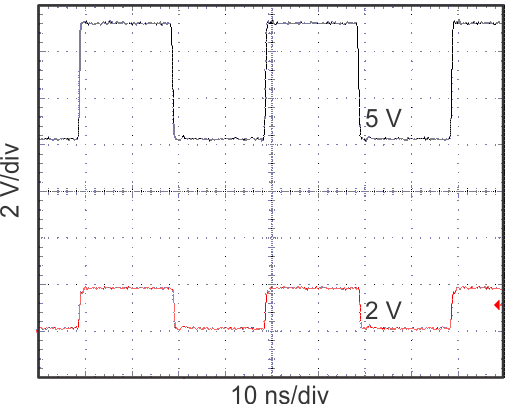
| VCCA = 1.8 V | VCCB = 5 V |