JAJSME3B March 2022 – January 2023 UCC21737-Q1
PRODUCTION DATA
- 1 特長
- 2 アプリケーション
- 3 概要
- 4 Revision History
- 5 Pin Configuration and Functions
-
6 Specifications
- 6.1 Absolute Maximum Ratings
- 6.2 ESD Ratings
- 6.3 Recommended Operating Conditions
- 6.4 Thermal Information
- 6.5 Power Ratings
- 6.6 Insulation Specifications
- 6.7 Safety Limiting Values
- 6.8 Electrical Characteristics
- 6.9 Switching Characteristics
- 6.10 Insulation Characteristics Curves
- 6.11 Typical Characteristics
- 7 Parameter Measurement Information
-
8 Detailed Description
- 8.1 Overview
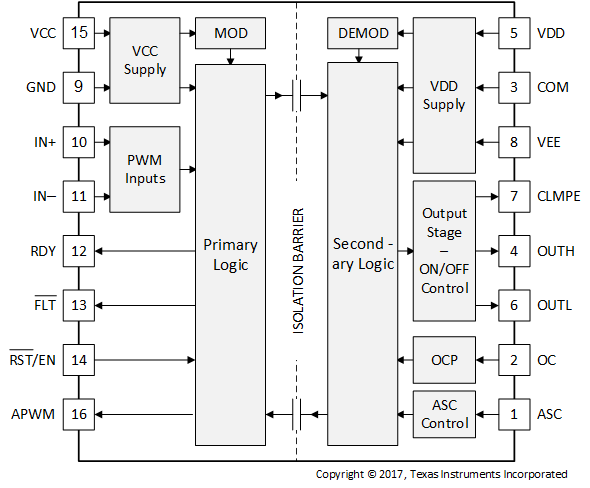
- 8.2 Functional Block Diagram
- 8.3
Feature Description
- 8.3.1 Power Supply
- 8.3.2 Driver Stage
- 8.3.3 VCC, VDD, and VEE Undervoltage Lockout (UVLO)
- 8.3.4 Active Pulldown
- 8.3.5 Short Circuit Clamping
- 8.3.6 External Active Miller Clamp
- 8.3.7 Overcurrent and Short Circuit Protection
- 8.3.8 Soft Turn-off
- 8.3.9 Fault (FLT), Reset, and Enable (RST/EN)
- 8.3.10 ASC Support and APWM Monitor
- 8.4 Device Functional Modes
-
9 Applications and Implementation
- 9.1 Application Information
- 9.2
Typical Application
- 9.2.1 Design Requirements
- 9.2.2
Detailed Design Procedure
- 9.2.2.1 Input Filters for IN+, IN-, and RST/EN
- 9.2.2.2 PWM Interlock of IN+ and IN-
- 9.2.2.3 FLT, RDY, and RST/EN Pin Circuitry
- 9.2.2.4 RST/EN Pin Control
- 9.2.2.5 Turnon and Turnoff Gate Resistors
- 9.2.2.6 External Active Miller Clamp
- 9.2.2.7 Overcurrent and Short Circuit Protection
- 9.2.2.8 Higher Output Current Using an External Current Buffer
- 9.2.3 Application Curves
- 10Power Supply Recommendations
- 11Layout
- 12Device and Documentation Support
- 13Mechanical, Packaging, and Orderable Information
パッケージ・オプション
メカニカル・データ(パッケージ|ピン)
- DW|16
サーマルパッド・メカニカル・データ
- DW|16
発注情報
3 概要
UCC21737-Q1 は、先進の保護機能、クラス最高の動的性能、堅牢性を持ち合わせ、最高 2121V (DC) で動作する SiC MOSFET および IGBT 用に設計されたガルバニック絶縁型シングル・チャネル・ゲート・ドライバです。本デバイスは最大 ±10A のピーク・ソース / シ ンク電流を供給できます。
入力側は SiO2 容量性絶縁技術によって出力側から絶縁され、最大 1.5kVRMS の動作電圧に対応し、40 年を超える寿命の絶縁バリアにより 12.8kVPK のサージ耐性を備えるとともに、部品間スキューが小さく、150V/ns を超える同相ノイズ耐性 (CMTI) を実現しています。
UCC21737-Q1 は、高速の過電流および短絡検出、シャント電流センシング、フォルト通知、アクティブ・ミラー・クランプ、入力側および出力側電源 UVLO などの最新の保護機能を備えているため、SiC および IGBT のスイッチング動作や堅牢性を最適化できます。ASC 機能を使用してシステム障害発生時にパワー・スイッチを強制的にオンにできるため、ドライバの汎用性をさらに高め、システム設計、サイズ、コストを簡素化できます。
製品情報
| 部品番号 (1) | パッケージ | 本体サイズ (公称) |
|---|---|---|
| UCC21737-Q1 | DW SOIC-16 | 10.3mm × 7.5mm |
(1) 利用可能なパッケージについては、このデータシートの末尾にある注文情報を参照してください。
デバイスのピン構成