JAJSR77 September 2023 UCC21738-Q1
PRODUCTION DATA
- 1
- 1 特長
- 2 アプリケーション
- 3 概要
- 4 Revision History
- 5 Pin Configuration and Functions
-
6 Specifications
- 6.1 Absolute Maximum Ratings
- 6.2 ESD Ratings
- 6.3 Recommended Operating Conditions
- 6.4 Thermal Information
- 6.5 Power Ratings
- 6.6 Insulation Specifications
- 6.7 Safety Limiting Values
- 6.8 Electrical Characteristics
- 6.9 Switching Characteristics
- 6.10 Insulation Characteristics Curves
- 6.11 Typical Characteristics
- 7 Parameter Measurement Information
-
8 Detailed Description
- 8.1 Overview
- 8.2 Functional Block Diagram
- 8.3
Feature Description
- 8.3.1 Power Supply
- 8.3.2 Driver Stage
- 8.3.3 VCC and VDD Undervoltage Lockout (UVLO)
- 8.3.4 Active Pulldown
- 8.3.5 Short Circuit Clamping
- 8.3.6 External Active Miller Clamp
- 8.3.7 Overcurrent and Short Circuit Protection
- 8.3.8 Soft Turn-off
- 8.3.9 Fault (FLT), Reset, and Enable (RST/EN)
- 8.3.10 ASC Support and APWM Monitor
- 8.4 Device Functional Modes
-
9 Applications and Implementation
- 9.1 Application Information
- 9.2
Typical Application
- 9.2.1 Design Requirements
- 9.2.2
Detailed Design Procedure
- 9.2.2.1 Input Filters for IN+, IN-, and RST/EN
- 9.2.2.2 PWM Interlock of IN+ and IN-
- 9.2.2.3 FLT, RDY, and RST/EN Pin Circuitry
- 9.2.2.4 RST/EN Pin Control
- 9.2.2.5 Turn-On and Turn-Off Gate Resistors
- 9.2.2.6 External Active Miller Clamp
- 9.2.2.7 Overcurrent and Short Circuit Protection
- 9.2.2.8 Higher Output Current Using an External Current Buffer
- 9.2.3 Application Curves
- 10Power Supply Recommendations
- 11Layout
- 12Device and Documentation Support
- 13Mechanical, Packaging, and Orderable Information
7.2 Input Deglitch Filter
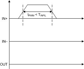
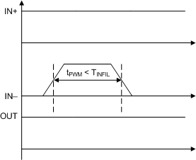
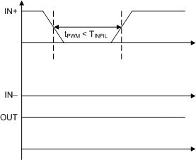
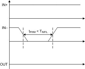
In order to increase the robustness of gate driver over noise transient and accidental small pulses on the input pins; that is, IN+, IN–, RST/EN, a 40-ns deglitch filter is designed to filter out the transients and make sure there is no faulty output responses or accidental driver malfunctions. When the IN+ or IN– PWM pulse is smaller than the input deglitch filter width, TINFIL, there will be no responses on OUT drive signal. Figure 7-3 and Figure 7-4 show the IN+ pin ON and OFF pulse deglitch filter effect. Figure 7-5 and Figure 7-6 show the IN– pin ON and OFF pulse deglitch filter effect.
 Figure 7-3 IN+
ON Deglitch Filter
 Figure 7-5 IN–
ON Deglitch Filter
 Figure 7-4 IN+
OFF Deglitch Filter
 Figure 7-6 IN–
OFF Deglitch Filter