JAJSHR2B september 2019 – october 2020 UCC23511
PRODUCTION DATA
- 1
- 1 特長
- 2 アプリケーション
- 3 概要
- 4 Revision History
- 5 Pin Configuration and Function
-
6 Specifications
- 6.1 Absolute Maximum Ratings
- 6.2 ESD Ratings
- 6.3 Recommended Operating Conditions
- 6.4 Thermal Information
- 6.5 Power Ratings
- 6.6 Insulation Specifications
- 6.7 Safety-Related Certifications
- 6.8 Safety Limiting Values
- 6.9 Electrical Characteristics
- 6.10 Switching Characteristics
- 6.11 Insulation Characteristics Curves
- 6.12 Typical Characteristics
- 7 Parameter Measurement Information
- 8 Detailed Description
- 9 Application and Implementation
- 10Power Supply Recommendations
- 11Layout
- 12Mechanical, Packaging, and Orderable Information
パッケージ・オプション
デバイスごとのパッケージ図は、PDF版データシートをご参照ください。
メカニカル・データ(パッケージ|ピン)
- DWY|6
サーマルパッド・メカニカル・データ
発注情報
9.2.2.4 Estimating Junction Temperature
Use Equation 10 to estimate the junction temperature (TJ) of UCC23511.
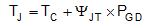
where
- TC is the UCC23511 case-top temperature measured with a thermocouple or some other instrument.
- ΨJT is the junction-to-top characterization parameter from the table.
Using the junction-to-top characterization parameter (ΨJT) instead of the junction-to-case thermal resistance (RθJC) can greatly improve the accuracy of the junction temperature estimation. The majority of the thermal energy of most ICs is released into the PCB through the package leads, whereas only a small percentage of the total energy is released through the top of the case (where thermocouple measurements are usually conducted). The RθJC resistance can only be used effectively when most of the thermal energy is released through the case, such as with metal packages or when a heat sink is applied to an IC package. In all other cases, use of RθJC will inaccurately estimate the true junction temperature. The ΨJT parameter is experimentally derived by assuming that the dominant energy leaving through the top of the IC will be similar in both the testing environment and the application environment. As long as the recommended layout guidelines are observed, junction temperature estimations can be made accurately to within a few degrees Celsius.