JAJSHM6E june 2019 – february 2021 UCC256402 , UCC256403 , UCC256404
PRODUCTION DATA
- 1
- 1 特長
- 2 アプリケーション
- 3 概要
- 4 Revision History
- Device Comparison Table
- 5 Pin Configuration and Functions
- 6 Specifications
-
7 Detailed Description
- 7.1 Overview
- 7.2 Functional Block Diagram
- 7.3 Feature Description
- 7.4 Device Functional Modes
-
Application and Implementation
- 8.1 Application Information
- 8.2
Typical Application
- 8.2.1 Design Requirements
- 8.2.2
Detailed Design Procedure
- 8.2.2.1 LLC Power Stage Requirements
- 8.2.2.2 LLC Gain Range
- 8.2.2.3 Select Ln and Qe
- 8.2.2.4 Determine Equivalent Load Resistance
- 8.2.2.5 Determine Component Parameters for LLC Resonant Circuit
- 8.2.2.6 LLC Primary-Side Currents
- 8.2.2.7 LLC Secondary-Side Currents
- 8.2.2.8 LLC Transformer
- 8.2.2.9 LLC Resonant Inductor
- 8.2.2.10 LLC Resonant Capacitor
- 8.2.2.11 LLC Primary-Side MOSFETs
- 8.2.2.12 LLC Rectifier Diodes
- 8.2.2.13 LLC Output Capacitors
- 8.2.2.14 HV Pin Series Resistors
- 8.2.2.15 BLK Pin Voltage Divider
- 8.2.2.16 ISNS Pin Differentiator
- 8.2.2.17 VCR Pin Capacitor Divider
- 8.2.2.18 BW Pin Voltage Divider
- 8.2.2.19 Soft Start and Burst Mode Programming
- 8.2.3 Application Curves
- 8 Power Supply Recommendations
- 9 Layout
- 10Device and Documentation Support
- Mechanical, Packaging, and Orderable Information
8.2.2.17 VCR Pin Capacitor Divider
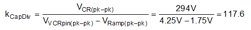
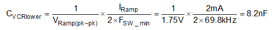
The capacitor divider on the VCR pin sets two parameters: (1) the divider ratio of the resonant capacitor voltage; (2) the amount of frequency compensation to be added. The first criteria the capacitor divider needs to meet is that under over load condition, the peak-to-peak voltage on the VCR pin is with in 6 V. It is recommended to size the VCR capacitance to give a total peak to peak voltage between 3 V and 4.5 V at full load with the frequency compensation ramp contributing between 1 V and 2 V to the total VCR peak to peak voltage. For this design, the VCR pin capacitance was selected to give a maximum peak to peak voltage of approximately 4.25 V at full load with the internal ramp contributing 1.75 V to the total VCR waveform.
The required VCR capacitance can be calculated directly from the resonant capacitor peak to peak voltage and the minimum expected switching frequency.

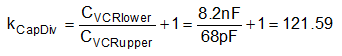
Based on the expected peak to peak resonant capacitor voltage, the required capacitor divider ratio can be derived
From the expected minimum switching frequency, the lower VCR capacitance can be derived
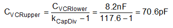
A standard value of 8.2 nF is chosen for the lower VCR capacitor. From the selected lower VCR capacitor and calculated capacitor divider ratio, the upper VCR capacitance is given by:
A standard value of 68 pF is selected for the upper VCR capacitor. From the selected upper and lower VCR capacitors, the actual peak to peak voltage on the VCR pin can be calculated