JAJSHM6E june 2019 – february 2021 UCC256402 , UCC256403 , UCC256404
PRODUCTION DATA
- 1
- 1 特長
- 2 アプリケーション
- 3 概要
- 4 Revision History
- Device Comparison Table
- 5 Pin Configuration and Functions
- 6 Specifications
-
7 Detailed Description
- 7.1 Overview
- 7.2 Functional Block Diagram
- 7.3 Feature Description
- 7.4 Device Functional Modes
-
Application and Implementation
- 8.1 Application Information
- 8.2
Typical Application
- 8.2.1 Design Requirements
- 8.2.2
Detailed Design Procedure
- 8.2.2.1 LLC Power Stage Requirements
- 8.2.2.2 LLC Gain Range
- 8.2.2.3 Select Ln and Qe
- 8.2.2.4 Determine Equivalent Load Resistance
- 8.2.2.5 Determine Component Parameters for LLC Resonant Circuit
- 8.2.2.6 LLC Primary-Side Currents
- 8.2.2.7 LLC Secondary-Side Currents
- 8.2.2.8 LLC Transformer
- 8.2.2.9 LLC Resonant Inductor
- 8.2.2.10 LLC Resonant Capacitor
- 8.2.2.11 LLC Primary-Side MOSFETs
- 8.2.2.12 LLC Rectifier Diodes
- 8.2.2.13 LLC Output Capacitors
- 8.2.2.14 HV Pin Series Resistors
- 8.2.2.15 BLK Pin Voltage Divider
- 8.2.2.16 ISNS Pin Differentiator
- 8.2.2.17 VCR Pin Capacitor Divider
- 8.2.2.18 BW Pin Voltage Divider
- 8.2.2.19 Soft Start and Burst Mode Programming
- 8.2.3 Application Curves
- 8 Power Supply Recommendations
- 9 Layout
- 10Device and Documentation Support
- Mechanical, Packaging, and Orderable Information
7.3.3.1 Optocoupler Feedback Signal Input and Bias
The secondary regulator circuit and optocoupler feedback circuit all add directly to the standby power consumed by the system. To achieve very low standby power it is necessary to drive the optocoupler in a low current mode.
As shown in Figure 7-3, a constant current source IFB is generated from VCC voltage and connected to FB pin. A resistor RFB is also connected to this current source with a PMOS in series. During normal operation, the PMOS is always on, so that the FB pin voltage will be equal to the zener diode reference voltage plus the voltage drop on the PMOS source to gate.
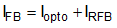
From this equation, when Iopto increases, IRFB will decrease, making FBreplica decrease. In this way, the control effort is inverted. A conventional way to bias the optocoupler is using a pull up resistor on the collector of the optocoupler output. To reduce the power consumption, the pull up resistor needs to be big, which will limit the loop bandwidth. For the bias current method used in UCC25640x, the FB pin voltage is maintained constant so that the parasitic capacitor of the optocoupler will not introduce an extra pole to the system, and subsequently limit the loop bandwidth.