JAJSHY6D September 2019 – October 2022 UCC27282-Q1
PRODUCTION DATA
- 1 特長
- 2 アプリケーション
- 3 概要
- 4 Revision History
- 5 Pin Configuration and Functions
- 6 Specifications
- 7 Detailed Description
- 8 Application and Implementation
- 9 Power Supply Recommendations
- 10Layout
- 11Device and Documentation Support
パッケージ・オプション
メカニカル・データ(パッケージ|ピン)
サーマルパッド・メカニカル・データ
発注情報
6.8 Typical Characteristics
Unless otherwise specified VVDD=VHB = 12 V, VHS=VVSS = 0 V, No load on outputs
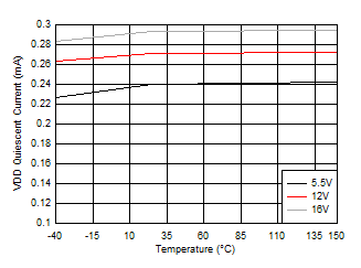
A.
Figure 6-1 VDD Quiescent Current| VHI = VLI = 0 V |
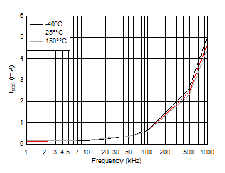 Figure 6-3 VDD Operating Current
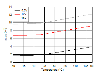
A.
Figure 6-5 VDD Current When Disabled| VEN = 0 V | ||
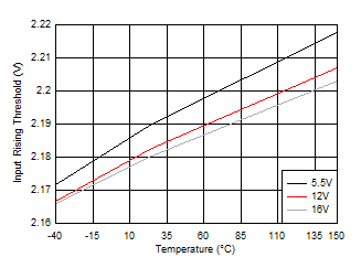 Figure 6-7 Input Rising Threshold
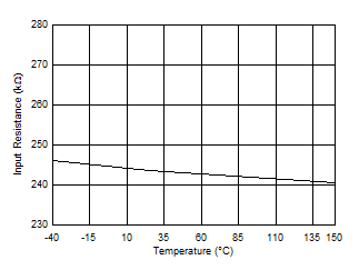 Figure 6-9 Input Pull-down Resistor
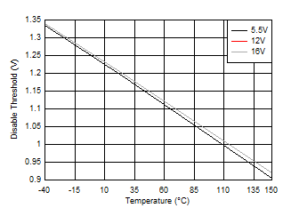 Figure 6-11 Disable Threshold
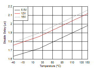 Figure 6-13 Disable Delay
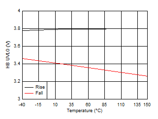 Figure 6-15 HB UVLO Threshold
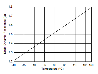 Figure 6-17 Boot Diode Dynamic Resistance
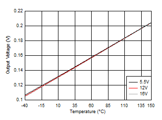
A.
Figure 6-19 LO High Output Voltage (VLOH)| IO=-100mA |
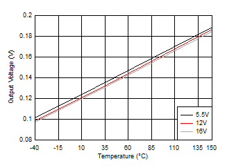
A.
Figure 6-21 HO High Output Voltage (VHOH)| IO=-100mA |
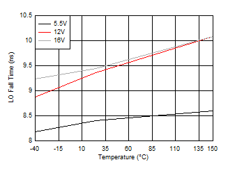
A.
Figure 6-23 LO Fall Time| CL=1800pF |
A.
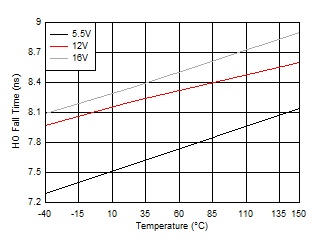
Figure 6-25 HO Fall Time| CL=1800pF |
A.
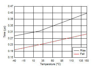
Figure 6-27 HO Rise & Fall Time| CL=100nF |
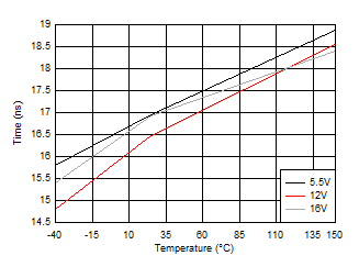 Figure 6-29 HO Falling Propagation Delay (TDHFF)
 Figure 6-31 LO Falling Propagation Delay (TDLFF)
A.
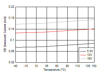
Figure 6-2 HB Quiescent Current| VHI = VLI = 0 V |
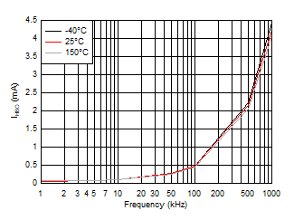 Figure 6-4 HB Operating Current
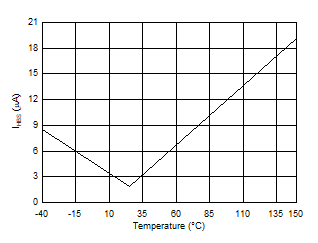
A.
Figure 6-6 HB to VSS Quiescent Current| VHB=VHS=100V |
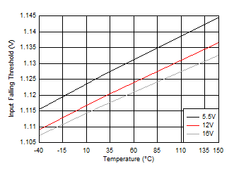
A.
Figure 6-8 Input Falling Threshold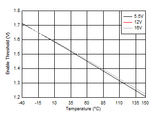 Figure 6-10 Enable Threshold
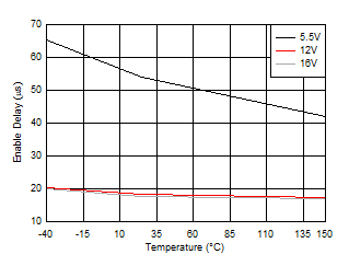 Figure 6-12 Enable Delay
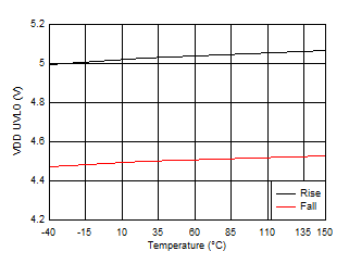 Figure 6-14 VDD UVLO Threshold
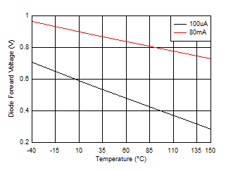 Figure 6-16 Boot Diode Forward Voltage Drop
A.
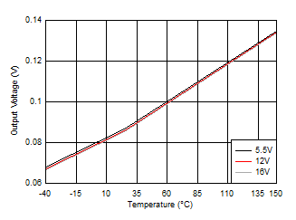
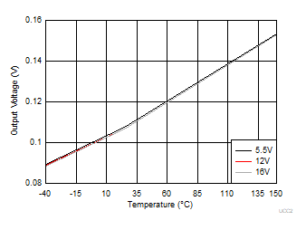
Figure 6-18 LO Low Output Voltage (VLOL)| IO=100mA |
A.
Figure 6-20 HO Low Output Voltage (VHOL)| IO=100mA |
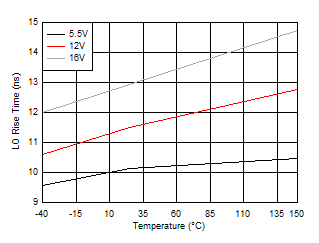
A.
Figure 6-22 LO Rise Time| CL=1800pF |
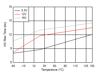
A.
Figure 6-24 HO Rise Time| CL=1800pF |
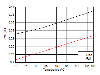
A.
Figure 6-26 LO Rise & Fall Time| CL=100nF |
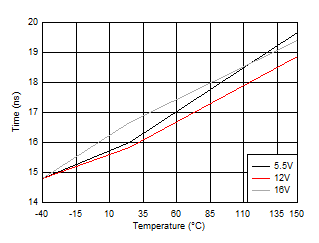 Figure 6-28 HO Rising Propagation Delay (TDHRR)
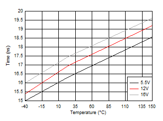 Figure 6-30 LO Rising Propagation Delay (TDLRR)