JAJS127E April 1999 – August 2016 UCC2813-0 , UCC2813-1 , UCC2813-2 , UCC2813-3 , UCC2813-4 , UCC2813-5 , UCC3813-0 , UCC3813-1 , UCC3813-2 , UCC3813-3 , UCC3813-4 , UCC3813-5
PRODUCTION DATA.
- 1 特長
- 2 アプリケーション
- 3 概要
- 4 改訂履歴
- 5 Device Comparison Table
- 6 Pin Configuration and Functions
- 7 Specifications
-
8 Detailed Description
- 8.1 Overview
- 8.2 Functional Block Diagram
- 8.3
Feature Description
- 8.3.1 Detailed Pin Descriptions
- 8.3.2 Undervoltage Lockout (UVLO)
- 8.3.3 Self-Biasing, Active Low Output
- 8.3.4 Reference Voltage
- 8.3.5 Oscillator
- 8.3.6 Synchronization
- 8.3.7 PWM Generator
- 8.3.8 Minimum Off-Time Adjustment (Dead-Time Control)
- 8.3.9 Leading Edge Blanking
- 8.3.10 Minimum Pulse Width
- 8.3.11 Current Limiting
- 8.3.12 Overcurrent Protection and Full-Cycle Restart
- 8.3.13 Soft Start
- 8.3.14 Slope Compensation
- 8.4 Device Functional Modes
-
9 Application and Implementation
- 9.1 Application Information
- 9.2
Typical Application
- 9.2.1 Design Requirements
- 9.2.2
Detailed Design Procedure
- 9.2.2.1 Bulk Capacitor Calculation
- 9.2.2.2 Transformer Design
- 9.2.2.3 MOSFET and Output Diode Selection
- 9.2.2.4 Output Capacitor Calculation
- 9.2.2.5 Current Sensing Network
- 9.2.2.6 Gate Drive Resistor
- 9.2.2.7 REF Bypass Capacitor
- 9.2.2.8 RT and CT
- 9.2.2.9 Start-Up Circuit
- 9.2.2.10 Voltage Feedback Compensation Procedure
- 9.2.3 Application Curves
- 10Power Supply Recommendations
- 11Layout
- 12デバイスおよびドキュメントのサポート
- 13メカニカル、パッケージ、および注文情報
パッケージ・オプション
デバイスごとのパッケージ図は、PDF版データシートをご参照ください。
メカニカル・データ(パッケージ|ピン)
- D|8
- PW|8
サーマルパッド・メカニカル・データ
発注情報
9 Application and Implementation
NOTE
Information in the following applications sections is not part of the TI component specification, and TI does not warrant its accuracy or completeness. TI’s customers are responsible for determining suitability of components for their purposes. Customers should validate and test their design implementation to confirm system functionality.
9.1 Application Information
The UCCx813-x controllers are peak-current-mode (PCM) pulse-width modulators (PWM). These controllers have an onboard amplifier and can be used in isolated and nonisolated power supply design. There is an onboard totem-pole gate driver capable of delivering up to ±1 A of peak current. These controllers are capable of operating at switching frequencies up to 1 MHz.
9.2 Typical Application
Figure 33 illustrates a typical circuit diagram for an AC-DC converter using the UCC2813-0 in a peak-current-mode-controlled flyback application.
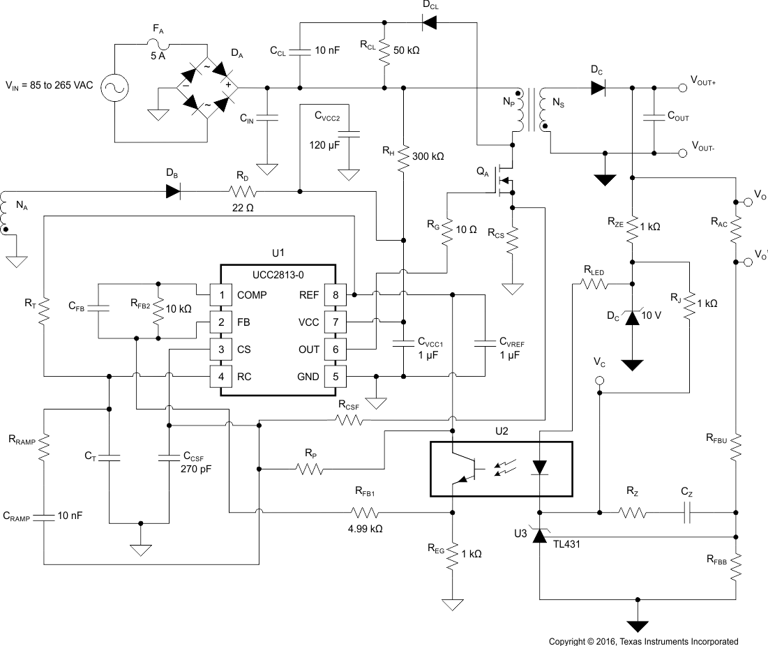 Figure 33. Typical Application Circuit Diagram
9.2.1 Design Requirements
Use the parameters in Table 2 to review the design of a 12-V, 48-W offline flyback converter using the UCC2813-0 PWM controller.
Table 2. Design Parameters
| PARAMETER | TEST CONDITIONS | MIN | NOM | MAX | UNIT | |
|---|---|---|---|---|---|---|
| INPUT CHARACTERSTICS | ||||||
| VIN | Input voltage (RMS) | 85 | 265 | V | ||
| fLINE | Line frequency | 47 | 63 | Hz | ||
| OUTPUT CHARACTRSTICS | ||||||
| VOUT | Output voltage | 11.75 | 12 | 12.25 | V | |
| Vripple | Output ripple voltage | 120 | mVPP | |||
| IOUT | Output current | 4 | 4.33 | A | ||
| Vtran | Output transient | Output voltage measured under 0-A to 4-A load step | 11.75 | 12.25 | V | |
| SYSTEM CHARACTRSTICS | ||||||
| η | Max load efficiency | 85% | ||||
9.2.2 Detailed Design Procedure
9.2.2.1 Bulk Capacitor Calculation
The design starts with selecting an appropriate bulk capacitor.
The primary-side bulk capacitor is selected based on the input power level and on the desired minimum bulk voltage level. The bulk capacitor value can be calculated by Equation 5.

where
- PIN is the maximum output power divided by the target efficiency at maximum load
- VIN(min) is the minimum AC input voltage RMS value
- VBULK(min) is the target minimum bulk voltage
- fLINE is the line frequency
Based on this equation, to achieve 75-V minimum bulk voltage, assuming 85% converter efficiency and 47-Hz minimum line frequency, the bulk capacitor must be larger than 127 µF. 180 µF was chosen in the design, considering the typical tolerance of bulk capacitors.
9.2.2.2 Transformer Design
The transformer design starts with selecting a suitable switching frequency. Generally the switching frequency selection is based on a tradeoff between the converter size and efficiency, based on the simple Flyback topology. Normally, higher switching frequency results in smaller transformer size. However, the switching loss is increased and hurts the efficiency. Sometimes, the switching frequency is selected to avoid certain communication bands to prevent noise interference with the communication. The frequency selection is beyond the scope of this data sheet.
The switching frequency is targeted for 110 kHz, to minimize the transformer size. At the same time, because EMI regulations start to limit conducted noise at 150 kHz, choosing 110-kHz switching frequency can help to reduce the EMI filter size.
The transformer turns ratio can be selected based on the desired MOSFET voltage rating and diode voltage rating. Because maximum input voltage is 265 V AC, the peak bulk voltage can be calculated by Equation 6.

To minimize the cost of the system, a popular 650-V MOSFET is selected. Considering the design margin and extra voltage ringing on the MOSFET drain, the reflected output voltage must be less than 120 V. The transformer turns ratio can be selected by Equation 7.

The transformer inductance selection is based on the continuous conduction mode (CCM) condition. Higher inductance would allow the converter to stay in CCM longer. However, it tends to increase the transformer size. Normally, the transformer magnetizing inductance is selected so that the converter enters CCM operation at about 50% load at minimum line voltage. This would be a tradeoff between the transformer size and the efficiency. In this particular design, due to the higher output current, it is desired to keep the converter deeper in CCM and minimize the conduction loss and output ripple. The converter enters CCM operation at about 10% load at minimum bulk voltage.
The inductor can be calculated as Equation 8.

In this equation, the switching frequency is 110 kHz. Therefore, the transformer inductance must be about 1.7 mH. 1.5 mH is chosen as the magnetizing inductance value.
The auxiliary winding provides the bias power for UCC2813-0 normal operation. The auxiliary winding voltage is the output voltage reflected to the primary side. It is desired to have higher reflected voltage so that the IC can quickly get energy from the transformer and make start-up under heavy load easier. However, higher reflected voltage makes the IC consume more power. Therefore, a tradeoff is required.
In this design, the auxiliary winding voltage is selected to be the same as the output voltage so that it is above the UVLO level but keeps the IC and driving loss low. Therefore, the auxiliary winding to the output winding turns ratio is selected by Equation 9.

Based on calculated primary inductance value and the switching frequency, the current stress of the MOSFET and diode can be calculated.
9.2.2.3 MOSFET and Output Diode Selection
The peak current of the MOSFET is calculated by Equation 10.

The MOSFET peak current is 1.425 A.
The RMS current of the MOSFET can be calculated as Equation 11.

where
- D is the MOSFET duty cycle at minimum bulk voltage and it can be calculated as Equation 12

The MOSFET RMS current is 0.75 A. With less than 0.9-Ω on-resistance, IRFB9N65A is selected as the primary-side MOSFET.
The diode peak current is the reflected MOSFET peak current on the secondary side.

The diode voltage stress is the output voltage plus the reflected input voltage. The voltage stress on the diode can be calculated by Equation 14.

Considering the ringing voltage spikes and voltage derating, the diode voltage rating must be higher than 50 V.
The diode average current is the output current (4 A), so 48CTQ060-1, with 60-V rating and 40-A average current capability, is selected.
9.2.2.4 Output Capacitor Calculation
The output capacitor is selected based on the output voltage ripple requirement. In this design, 0.1% voltage ripple is assumed. Based on the 0.1% ripple requirement, the capacitor value can be selected based on Equation 15.

Considering the tolerance and temperature effect, together the ripple current rating of the capacitors, 3 parallel 680-µF capacitors are selected for the output.
After the basic power stage is designed, the surrounding controller components can be selected.
9.2.2.5 Current Sensing Network
The current sensing network consists of RCS, RCSF, CCSF, and optional RP. Typically, the direct current sense signal contains a large-amplitude leading-edge spike associated with the turn-on of the main power MOSFET, reverse recovery of the output rectifier, and other factors including charging and discharging of parasitic capacitances. Therefore, CCSF and RCSF form a low-pass filter that provides additional immunity beyond the internal blanking time to suppress the leading edge spike. For this converter, CCSF is chosen to be 270 pF to provide enough filtering.
Without RP, RCS sets the maximum peak current in the transformer primary based on the maximum amplitude of CS pin, 1 V. To achieve 1.425-A primary side peak current, a 0.75-Ω resistor is chosen for RCS.
The high current-sense threshold helps to provide better noise immunity but the current-sense loss is increased. The current-sense loss can be minimized by injecting an offset voltage into the current-sense signal. RP and RCSF form a resistor-divider network from the current-sense signal to the device’s reference voltage to offset the current-sense voltage. This technique still achieves current-mode control with cycle-by-cycle overcurrent protection. To calculate required offset value (Voffset), use Equation 16.

9.2.2.6 Gate Drive Resistor
RG is the gate driver resistor for the power switch, QA. The selection of this resistor value must be done in conjunction with EMI compliance testing and efficiency testing. Larger RG slows down the turn-on and turn-off of the MOSFET. Slower switching speed reduces EMI but also increases the switching loss. A tradeoff between switching loss and EMI performance must be carefully performed. For this design, 10 Ω was chosen as the gate driver resistor.
9.2.2.7 REF Bypass Capacitor
The precision 5-V reference voltage at REF is designed to perform several important functions. The reference voltage is divided down internally to 2.5 V and connected to the error amplifier’s noninverting input for accurate output voltage regulation. Other duties of the reference voltage are to set internal bias currents and thresholds for functions such as the oscillator upper and lower thresholds along with the overcurrent limiting threshold. Therefore, the reference voltage must be bypassed with a ceramic capacitor (CVREF), and 1-µF, 16-V ceramic capacitor was selected for this converter. Placement of this capacitor on the physical printed-circuit board layout must be as close as possible to the respective REF and GND pins.
9.2.2.8 RT and CT
The internal oscillator uses a timing capacitor (CT) and a timing resistor (RT) to program operating frequency and maximum duty cycle. The operating frequency can be programmed based the curves in Figure 3, where the timing resistor can be found once the timing capacitor is selected. The selection of timing capacitor also affects the maximum duty cycle provided in Figure 5. It is best for the timing capacitor to have a flat temperature coefficient, typical of most COG or NPO type capacitors. For this converter, 1000 pF and 13.6 kΩ were selected for CT and RT to operate at 110-kHz switching frequency.
9.2.2.9 Start-Up Circuit
At start-up, the IC gets its power directly from the high voltage bulk, through a high-voltage resistor RH. The selection of start-up resistor is the tradeoff between power loss and start-up time. The current flowing through RH at minimum input voltage must be higher than the VCC current under UVLO condition (0.2 mA at its maximum value). A 300-kΩ resistor is chosen as the result of the tradeoff.
After VCC is charged up above the UVLO turnon threshold, UCC2813-0 starts to operate and consumes full operating current. At the beginning, because the output voltage is low, VCC cannot get energy from the auxiliary winding. The VCC capacitor is required to hold enough energy to prevent its voltage drop below UVLO during the start-up time, until the output reaches high enough. A larger capacitor holds more energy but slows down the start-up time. In this design, a 120-µF capacitor is chosen to provide enough energy for the start-up purpose.
9.2.2.10 Voltage Feedback Compensation Procedure
Feedback compensation, also called closed-loop control, reduces or eliminates steady-state output voltage error, reduces the sensitivity to parametric changes, changes the gain or phase of a system over some desired frequency range, reduces the effects of small-signal load disturbances and noise on system performance, and creates a stable system. This section describes how to compensate an isolated Flyback converter with the peak-current-mode control.
9.2.2.10.1 Power Stage Gain, Zeroes, and Poles
The first step in compensating a fixed-frequency flyback is to verify if the converter operates in continuous conduction mode (CCM) or discontinuous conduction mode (DCM). If the primary inductance (LP) is greater than the inductance for DCM-CCM boundary mode operation, called the critical inductance (LPcrit), then the converter operates in CCM. LPcrit is calculated with Equation 17.

For loads greater than 10% of PMAX over the entire input voltage range, the selected primary inductance has value larger than the critical inductance. Therefore, the converter operates in CCM and the compensation loop requires design based on CCM flyback equations.
The current-to-voltage conversion is done externally with the ground-referenced current-sense resistor (RCS) and the internal resistor divider sets up the internal current-sense gain, ACS = 1.65. The IC technology allows tight control of the resistor-divider ratio, regardless of the actual resistor value variations.
The DC open-loop gain (GO) of the fixed-frequency voltage control loop of a peak-current-mode control CCM flyback converter shown in Figure 33 is approximated by first using the output load (ROUT), the primary to secondary turns ratio (NPS), and the maximum duty cycle (D) as shown in Equation 18.

where
- ROUT = VOUT / IOUT
- D is calculated with Equation 19
- τL is calculated with Equation 20
- M is calculated with Equation 21


For this design, a converter with an output voltage (VOUT) of 12 V, and 48 W relates to an output load (ROUT) equal to 3 Ω at full load.
At minimum input bulk voltage of 75 V DC, the duty cycle reaches its maximum value of 0.615. The current sense resistance (RCS) is 0.75 Ω and a primary to secondary turns-ratio (NPS) is 10. The open-loop gain calculates to 14.95 dB.
A CCM flyback transfer function has two zeroes that are of interest. The ESR and the output capacitance contribute a left-half plane zero to the power stage, and the frequency of this zero (fESRz) is calculated with Equation 22.

The fESRz zero for a capacitance bank of three 680-µF capacitors (for a total output capacitance of 2040 µF) and a total ESR of 13 mΩ is located at 6 kHz.
CCM flyback converters have a zero in the right-half plane (RHP) of their transfer function. RHP zero has the same 20 dB/decade rising gain magnitude with increasing frequency just like a left-half plane zero, but it adds phase lag instead of lead. This phase lag tends to limit the overall loop bandwidth. The frequency location (fRHPz) in Equation 23 is a function of the output load, the duty cycle, the primary inductance (LP), and the primary to secondary side turns ratio (NPS).

RHP zero frequency increases with higher input voltage and lighter load. Generally, the design requires consideration of the worst case of the lowest RHP zero frequency and the converter must be compensated at the minimum input and maximum load condition. With a primary inductance of 1.5 mH, at 75-V DC input, the RHP zero frequency (fRHPz) is equal to 7.65 kHz at maximum duty cycle (full load).
The power stage has one dominant pole (ωP1) which is in the region of interest, located at a lower frequency (fP1) which is related to the duty cycle (D), the output load, and the output capacitance. There is also a double pole (fP2) located at half the switching frequency of the converter. These poles are frequencies calculated with Equation 24 and Equation 25.


Subharmonic oscillation is the large signal instability that can occur in CCM flyback converters when duty cycles extend beyond 50%. The subharmonic oscillation increases the output voltage ripple and sometimes it even limits the power handling capability of the converter. Slope compensation to the CS signal is a technique used to eliminate the instability.
Ideally, the target of slope compensation is to achieve quality coefficient (QP = 1) at half of the switching frequency. The QP is calculated by Equation 26.

where
- D is the primary side switch duty cycle
- MC is the slope compensation factor, which is defined by Equation 27

where
- Se is the compensation ramp slope
- Sn represents the rising current slope of the transformer primary inductance
The optimal goal of the slope compensation is to achieve QP equal to 1, which means MC must be 2.128 when D reaches it maximum value of 0.615.
The inductance current slope at the CS pin is calculated by Equation 28.

The compensation slope is calculated by Equation 29.

The compensation slope is added into the system through RRAMP and RCSF. A series capacitor (CRAMP) is selected to approximate a high-frequency short circuit. Choose CRAMP as 10 nF as the starting point, and make adjustments if required. RRAMP and RCSF form a voltage divider to scale the RC pin ramp voltage and inject the slope compensation into CS pin. Choose RRAMP much larger than the RT resistor so that it does not affect the frequency setting very much. In this design, RRAMP is selected as 24.9 kΩ. The RC pin ramp slope is calculated with Equation 30.

To achieve 46.3 mV/µs compensation slope, RCSF resistor is calculated with Equation 31.

The power stage open-loop gain and phase can be plotted as a function of frequency. The total open-loop transfer function, as a function of frequency, can be characterized by Equation 32.

where
- ωP1 and ωP2 are based on the frequencies calculated by Equation 24 and Equation 25
The open-loop gain and phase Bode plots are graphed accordingly (see Figure 34 and Figure 35).
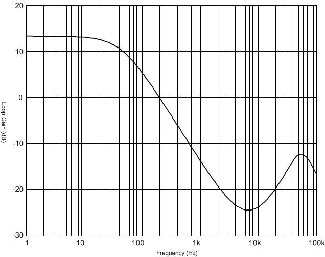 Figure 34. Converter Open-Loop Bode Plot: Gain
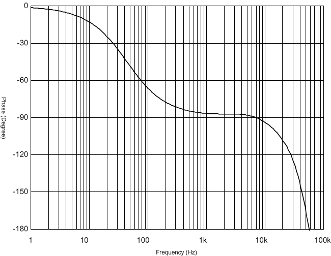 Figure 35. Converter Open-Loop Bode Plot: Phase
9.2.2.10.2 Compensating the Loop
For good transient response, the bandwidth of the finalized design must be as wide as possible. The bandwidth of a CCM flyback (fBW) is limited to ¼ of the RHP-zero frequency, or approximately 1.9 kHz using Equation 33.

The gain of the open-loop power stage at fBW is equal to –22.4 dB and the phase at fBW is equal to –87°. First step is to choose the output voltage-sensing resistor values. The output sensing resistors are selected based on the allowed power consumption and in this case, 1 mA of sensing current is assumed.
The TL431 is used as the feedback amplifier. Given its 2.5-V reference voltage, the voltage-sensing dividers RFBU and RFBB can be selected with Equation 34 and Equation 35.


Next step is to put the compensator zero fCZ at 190 Hz, which is 1/10 of the target crossover frequency. Choose CZ as a fixed value of 10 nF and choose the zero resistor value according to Equation 36.

Next, place a pole at the lower of RHP-zero or the ESR-zero frequencies. Based previous analysis, the RHP zero is at 7.65 kHz and the ESR zero is at 6 kHz, so the pole of the compensation loop should be put at 6 kHz. This pole can be added through the primary side error amplifier. RFB and CFB provide the necessary pole. Choosing RFB as 10 kΩ, CFB is calculated by Equation 37.

Based on the compensation loop structure, the entire compensation loop transfer function is written as Equation 38.

where
- CTR is the current transfer ratio of the opto-coupler. Choose 1 as the nominal value for CTR.
- REG is the opto-emitter pulldown resistor and 1 kΩ is chosen as a default value
The only remaining unknown value required in this equation is RLED. The entire loop gain must be equal to 1 at the crossover frequency. RLED is calculated accordingly as 1.62 kΩ.
The final closed-loop Bode plots are shown in Figure 36 and Figure 37. The converter achieves approximately 2-kHz crossover frequency and approximately 70° of phase margin.
TI recommends checking the loop stability across all the corner cases, including component tolerances, to ensure system stability.
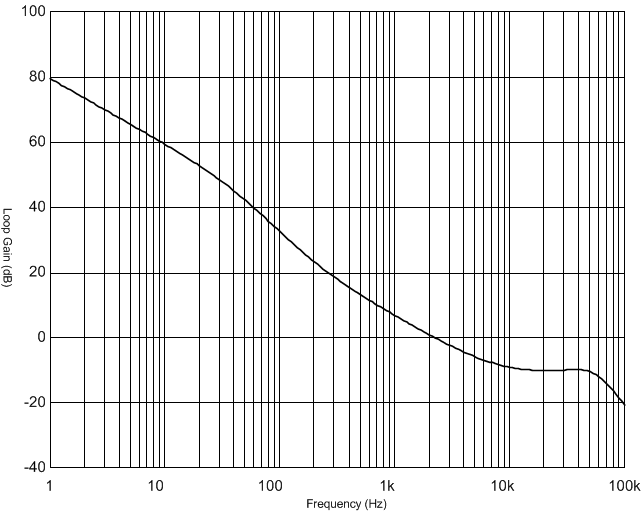 Figure 36. Converter Closed-Loop Bode Plot: Gain
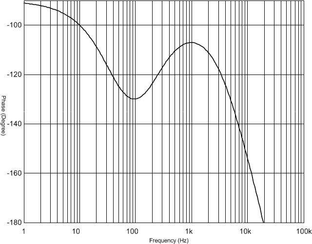 Figure 37. Converter Closed-Loop Bode Plot: Phase
9.2.3 Application Curves
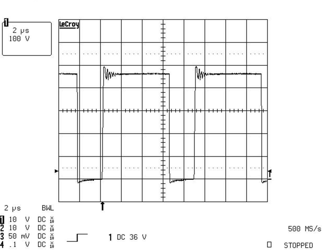
| 100 V/div | 2 µs/div |
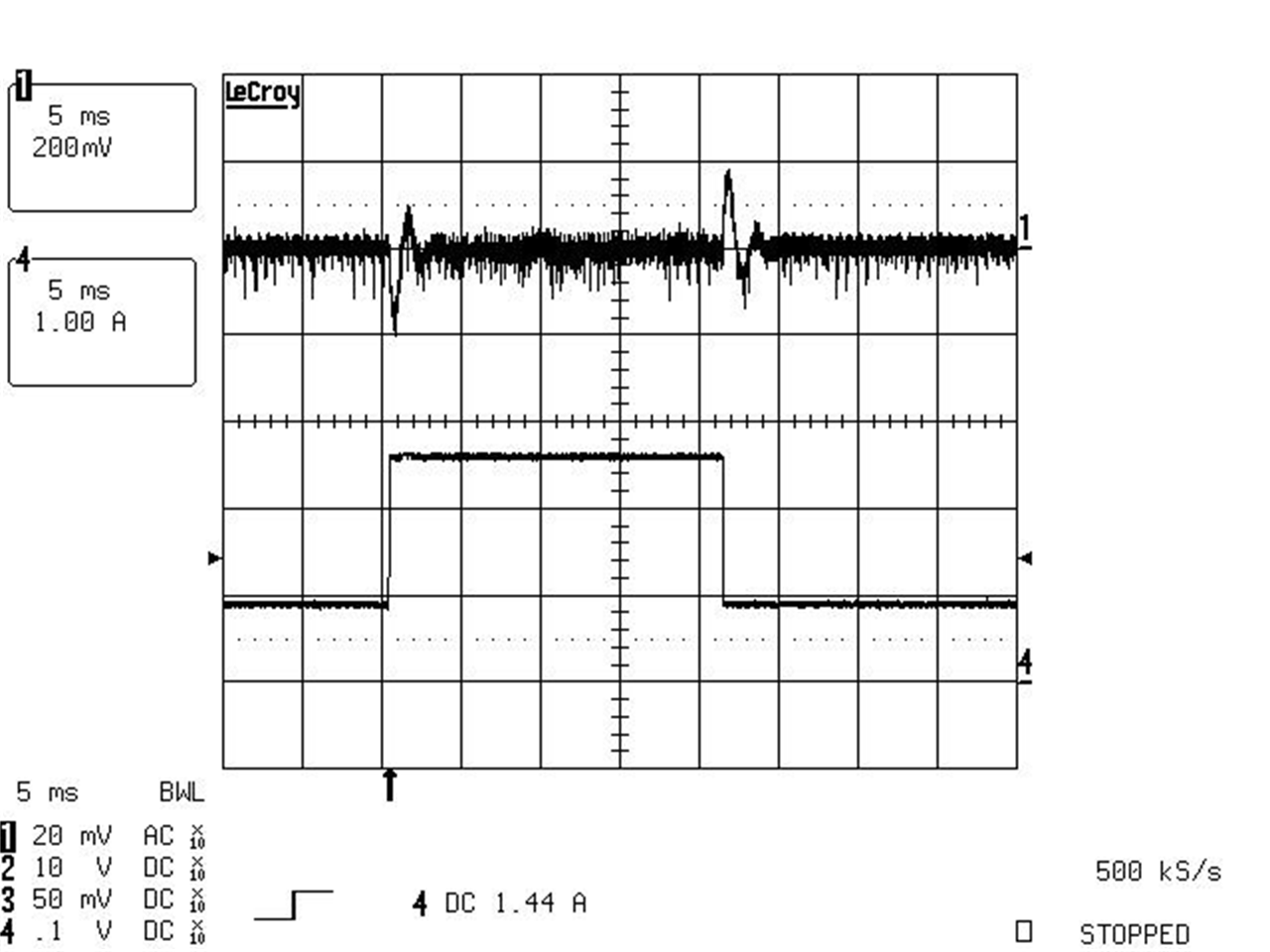
| CH1: output voltage AC coupled | 200 mV/div | |
| CH4: output current | 1 A/div | 5 ms/div |
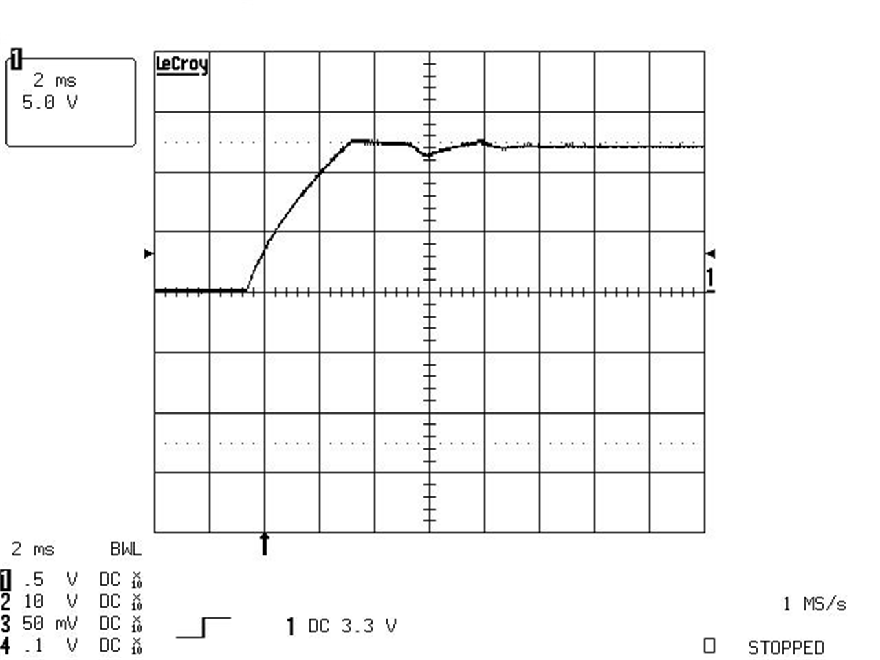
| 5 V/div | 2 ms/div |
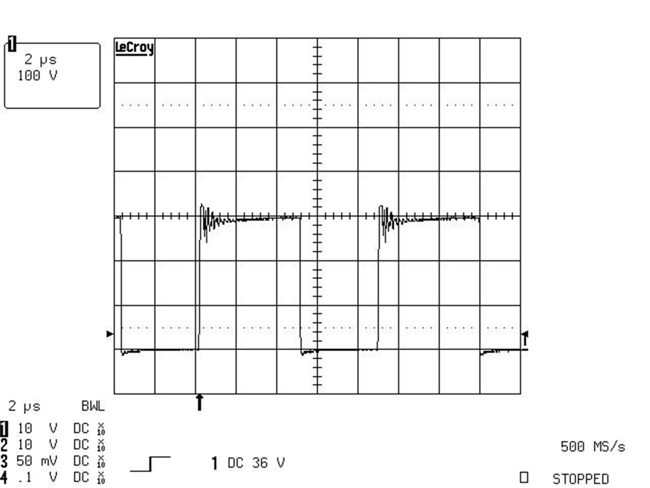
| 100 V/div | 2 µs/div |
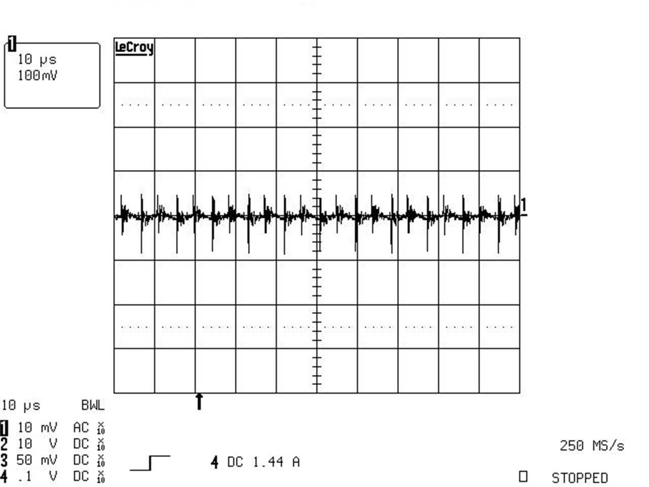
| 100 mV/div | 10 µs/div | |