JAJS124Q December 1999 – October 2019 UCC1895 , UCC2895 , UCC3895
PRODUCTION DATA.
- 1 特長
- 2 アプリケーション
- 3 概要
- 4 改訂履歴
- 5 Pin Configuration and Functions
- 6 Specifications
-
7 Detailed Description
- 7.1 Overview
- 7.2 Functional Block Diagrams
- 7.3
Feature Description
- 7.3.1 ADS (Adaptive Delay Set)
- 7.3.2 CS (Current Sense)
- 7.3.3 CT (Oscillator Timing Capacitor)
- 7.3.4 DELAB and DELCD (Delay Programming Between Complementary Outputs)
- 7.3.5 EAOUT, EAP, and EAN (Error Amplifier)
- 7.3.6 OUTA, OUTB, OUTC, and OUTD (Output MOSFET Drivers)
- 7.3.7 PGND (Power Ground)
- 7.3.8 RAMP (Inverting Input of the PWM Comparator)
- 7.3.9 REF (Voltage Reference)
- 7.3.10 RT (Oscillator Timing Resistor)
- 7.3.11 GND (Analog Ground)
- 7.3.12 SS/DISB (Soft Start/Disable)
- 7.3.13 SYNC (Oscillator Synchronization)
- 7.3.14 VDD (Chip Supply)
- 7.4 Device Functional Modes
- 7.5 Programming
-
8 Application and Implementation
- 8.1 Application Information
- 8.2
Typical Application
- 8.2.1 Design Requirements
- 8.2.2
Detailed Design Procedure
- 8.2.2.1 Power Loss Budget
- 8.2.2.2 Preliminary Transformer Calculations (T1)
- 8.2.2.3 QA, QB, QC, QD FET Selection
- 8.2.2.4 Selecting LS
- 8.2.2.5 Selecting Diodes DB and DC
- 8.2.2.6 Output Inductor Selection (LOUT)
- 8.2.2.7 Output Capacitance (COUT)
- 8.2.2.8 Select Rectifier Diodes
- 8.2.2.9 Input Capacitance (CIN)
- 8.2.2.10 Current Sense Network (CT, RCS, RR, DA)
- 8.2.3 Application Curves
- 9 Power Supply Recommendations
- 10Layout
- 11デバイスおよびドキュメントのサポート
- 12メカニカル、パッケージ、および注文情報
パッケージ・オプション
メカニカル・データ(パッケージ|ピン)
サーマルパッド・メカニカル・データ
発注情報
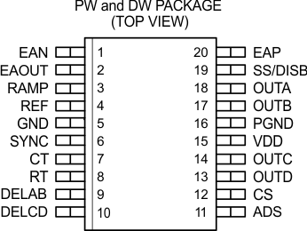
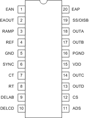
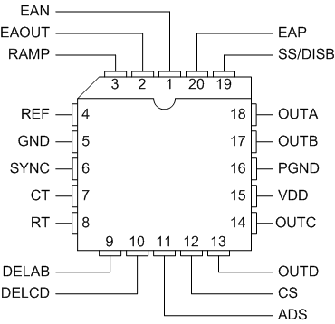
5 Pin Configuration and Functions
PW AND DW PACKAGE DRAWINGS
(TOP VIEW)

N AND J PACKAGE DRAWINGS
(TOP VIEW)

FN AND FK PACKAGE DRAWINGS
(TOP VIEW)

Pin Functions
| PIN | I/O | DESCRIPTION | |
|---|---|---|---|
| NAME | NO. | ||
| ADS | 11 | I | The adaptive-delay-set pin sets the ratio between the maximum and minimum programmed output delay dead time. |
| CS | 12 | I | Current sense input for cycle-by-cycle current limiting and for over-current comparator. |
| CT | 7 | I | Oscillator timing capacitor for programming the switching frequency. The UCC3895 oscillator charges CT via a programmed current. |
| DELAB | 9 | I | The delay-programming between complementary-outputs pin, DELAB, programs the dead time between switching of output A and output B. |
| DELCD | 10 | I | The delay-programming between complementary-outputs pin, DELCD, programs the dead time between switching of output C and output D. |
| EAOUT | 2 | I/O | Error amplifier output. |
| EAP | 20 | I | Non-inverting input to the error amplifier. Keep below 3.6 V for proper operation. |
| EAN | 1 | I | Inverting input to the error amplifier. Keep below 3.6 V for proper operation. |
| GND | 5 | — | Chip ground for all circuits except the output stages. |
| OUTA | 18 | O | The four outputs are 100-mA complementary MOS drivers, and are optimized to drive FET driver circuits such as UCC27714 or gate drive transformers. |
| OUTB | 17 | O | |
| OUTC | 14 | O | |
| OUTD | 13 | O | |
| PGND | 16 | — | Output stage ground. |
| RAMP | 3 | I | Inverting input of the PWM comparator. |
| REF | 4 | O | 5-V, ±1.2%, 5-mA voltage reference. For best performance, bypass with a 0.1-μF low ESR, low ESL capacitor to ground. Do not use more than 4.7 μF of total capacitance on this pin. |
| RT | 8 | I | Oscillator timing resistor for programming the switching frequency. |
| SS/DISB | 19 | I | Soft-start and disable pin which combines the two independent functions. |
| SYNC | 6 | I/O | The oscillator synchronization pin is bidirectional. |
| VDD | 15 | I | The power supply input pin, VDD, must be bypassed with a minimum of a 1-μF low ESR, low ESL capacitor to ground. The addition of a 10-μF low ESR, low ESL between VDD and PGND is recommended. |