SLUSDV5B October   2019  – April 2020 UCC5304

PRODUCTION DATA.  

  1. Features
  2. Applications
  3. Description
    1.     Device Images
      1.      Typical Application
  4. Revision History
  5. Pin Configuration and Functions
    1.     Pin Functions
  6. Specifications
    1. 6.1  Absolute Maximum Ratings
    2. 6.2  ESD Ratings
    3. 6.3  Recommended Operating Conditions
    4. 6.4  Thermal Information
    5. 6.5  Power Ratings
    6. 6.6  Insulation Specifications
    7. 6.7  Safety-Related Certifications
    8. 6.8  Safety-Limiting Values
    9. 6.9  Electrical Characteristics
    10. 6.10 Switching Characteristics
    11. 6.11 Typical Characteristics
  7. Parameter Measurement Information
    1. 7.1 Rising and Falling Time
    2. 7.2 Power-up UVLO Delay to OUTPUT
  8. Detailed Description
    1. 8.1 Overview
    2. 8.2 Functional Block Diagram
    3. 8.3 Feature Description
      1. 8.3.1 VDD, VCCI, and Under Voltage Lock Out (UVLO)
      2. 8.3.2 Input Stage
      3. 8.3.3 Output Stage
    4. 8.4 Device Functional Modes
  9. Application and Implementation
    1. 9.1 Application Information
    2. 9.2 Typical Application
      1. 9.2.1 Design Requirements
      2. 9.2.2 Detailed Design Procedure
        1. 9.2.2.1 Designing IN pin Input Filter
        2. 9.2.2.2 Estimating Junction Temperature
        3. 9.2.2.3 Selecting VCCI and VDD Capacitors
          1. 9.2.2.3.1 Selecting a VCCI Capacitor
          2. 9.2.2.3.2 Selecting a VDD Capacitor
  10. 10Power Supply Recommendations
  11. 11Layout
    1. 11.1 Layout Guidelines
      1. 11.1.1 Component Placement Considerations
      2. 11.1.2 Grounding Considerations
      3. 11.1.3 High-Voltage Considerations
      4. 11.1.4 Thermal Considerations
    2. 11.2 Layout Example
  12. 12Mechanical, Packaging, and Orderable Information

パッケージ・オプション

メカニカル・データ(パッケージ|ピン)
サーマルパッド・メカニカル・データ
発注情報

Mechanical, Packaging, and Orderable Information

The following pages include mechanical, packaging, and orderable information. This information is the most current data available for the designated devices. This data is subject to change without notice and revision of this document. For browser-based versions of this data sheet, refer to the left-hand navigation.
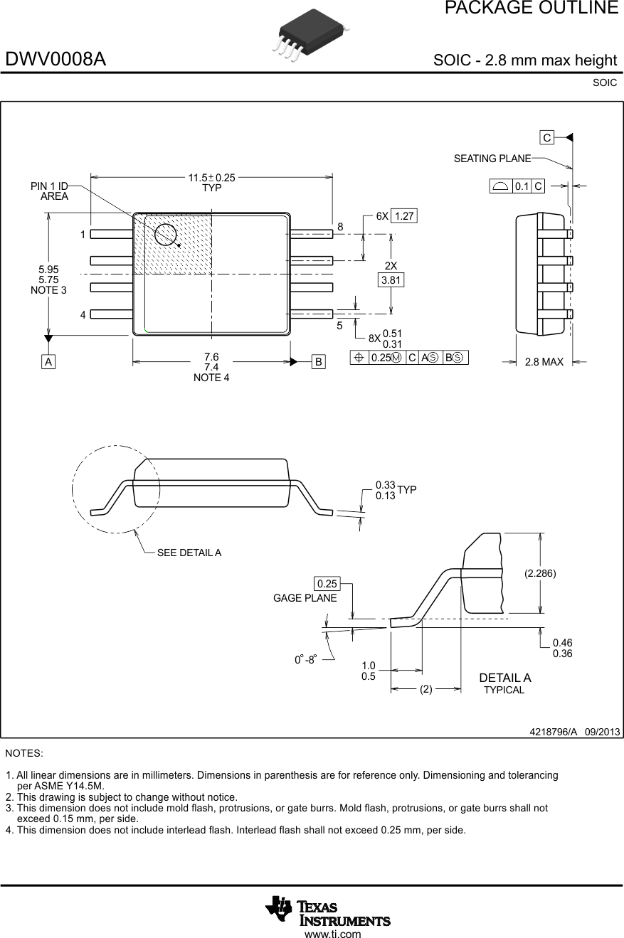
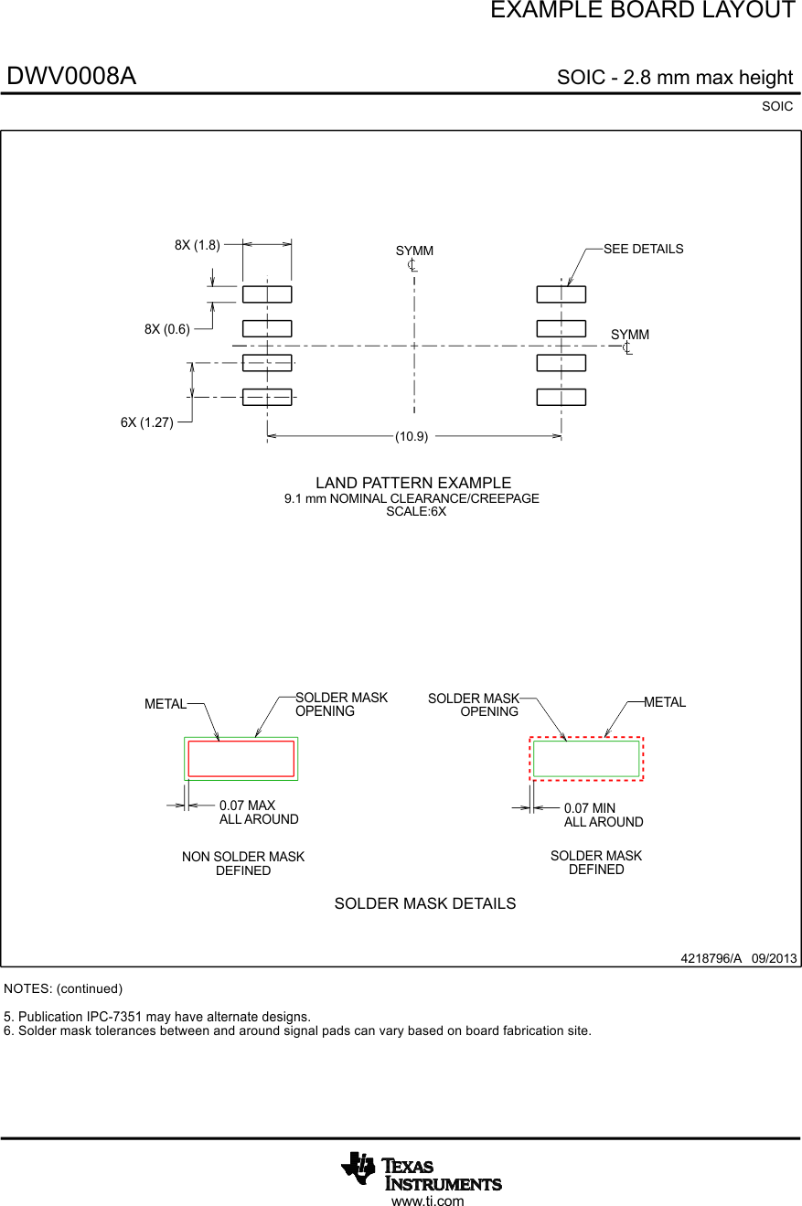
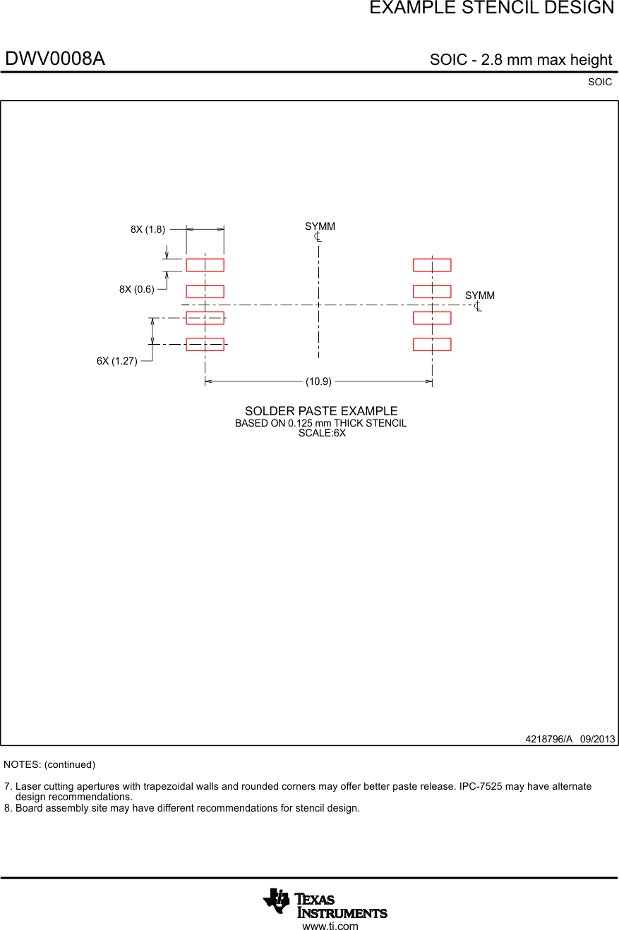
UCC5304 DWV0008A_4218796_Page_01.gif
UCC5304 DWV0008A_4218796_Page_02.gif
UCC5304 DWV0008A_4218796_Page_03.gif