SLUSDV5B October 2019 – April 2020 UCC5304
PRODUCTION DATA.
- 1 Features
- 2 Applications
- 3 Description
- 4 Revision History
- 5 Pin Configuration and Functions
-
6 Specifications
- 6.1 Absolute Maximum Ratings
- 6.2 ESD Ratings
- 6.3 Recommended Operating Conditions
- 6.4 Thermal Information
- 6.5 Power Ratings
- 6.6 Insulation Specifications
- 6.7 Safety-Related Certifications
- 6.8 Safety-Limiting Values
- 6.9 Electrical Characteristics
- 6.10 Switching Characteristics
- 6.11 Typical Characteristics
- 7 Parameter Measurement Information
- 8 Detailed Description
- 9 Application and Implementation
- 10Power Supply Recommendations
- 11Layout
- 12Mechanical, Packaging, and Orderable Information
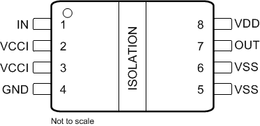
5 Pin Configuration and Functions
DWV Package
8-Pin SOIC
Top View

Pin Functions
| PIN | I/O(1) | DESCRIPTION | |
|---|---|---|---|
| GND | 4 | P | Primary-side ground reference. All signals in the primary side are referenced to this ground. |
| IN | 1 | I | Input signal. IN input has a TTL/CMOS compatible input threshold. This pin is pulled low internally if left open. It is recommended to tie this pin to ground if not used to achieve better noise immunity. |
| OUT | 7 | O | Output of driver. Connect to the gate of the FET or IGBT. |
| VCCI | 2, 3 | P | Primary-side supply voltage. Locally decoupled to GND using a low ESR/ESL capacitor located as close to the device as possible. |
| VDD | 8 | P | Secondary-side power for driver. Locally decoupled to VSS using a low ESR/ESL capacitor located as close to the device as possible. |
| VSS | 5, 6 | P | Ground for secondary-side driver. |
(1) P = power, G = ground, I = input, O = output