SLUS645F February 2005 – December 2014 UCD7201
PRODUCTION DATA.
- 1 Features
- 2 Applications
- 3 Description
- 4 Revision History
- 5 Description (Continued)
- 6 Pin Configuration and Functions
- 7 Specifications
- 8 Detailed Description
- 9 Applications and Implementation
- 10Power Supply Recommendations
- 11Layout
- 12Device and Documentation Support
- 13Mechanical, Packaging, and Orderable Information
パッケージ・オプション
メカニカル・データ(パッケージ|ピン)
- PWP|14
サーマルパッド・メカニカル・データ
- PWP|14
発注情報
9 Applications and Implementation
NOTE
Information in the following applications sections is not part of the TI component specification, and TI does not warrant its accuracy or completeness. TI’s customers are responsible for determining suitability of components for their purposes. Customers should validate and test their design implementation to confirm system functionality.
9.1 Application Information
The UCD7201 is member of the UCD7K family of digital compatible drivers targeting applications utilizing digital control techniques or applications that require local fast peak current limit protection.
9.2 Typical Applications
9.2.1 Half-Bridge Converter
Figure 25 shows the UCD7201 in a half-bridge converter design. The digital controller is performing the output voltage compensation and all supervisory functions. The isolation amplifier is made up of a linear opto-coupler configured for a gain of 1/10, so the output voltage is transformed to a level comparable with the ADC of the digital controller.
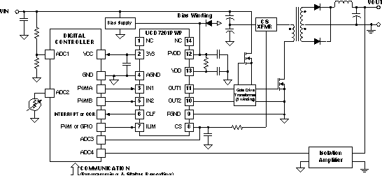 Figure 25. Half-Bridge Converter
9.2.1.1 Design Requirements
In this design example, the input current is sensed by a current transformer (CT), the cycle-by-cycle protection threshold is set at 5 A.
9.2.1.2 Detailed Design Procedure
The cycle-by-cycle current protection is implemented by connect the current sense signal to CS pin. When the CS level is greater than the ILIM voltage minus 25 mV, the output of the driver is forced low and the current limit flag (CLF) is set high. The CLF signal is latched high until the UCD7K device receives the next rising edge on the IN pin.
The current limit threshold can be set to any value between 0.25 V and 1.0 V, select the right turns ratio of the CT and right resistor at the output of CT, such that the CT output is within this range. Assuming the CT output is 0.775V when input current is 5A, if the digital controller has internal digital-to-analog converter, then it can generate 0.775 V and connect to ILIM directly. For digital controller without internal digital-to-analog converter, it can generate PWM signal, send PWM signal through a low pass filter, then connect to ILIM pin.
Assuming the magnitude of the PWM pulse is 3.3V, then the duty cycle is:

9.2.1.3 Application Curves
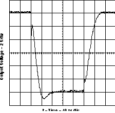 Figure 26. Output Rise and Fall Time (VDD = 12 V, CLOAD = 10 nF)
9.2.2 Intermediate Bus Converter
Figure 27 shows the UCD7201 in an analog only implementation of an intermediate bus converter. The ILIM pin of the UCD7201 is exponentially increased at start-up, which minimizes overshoot on the output voltage. The UCC28089 is a push-pull controller with fixed dead-time. The UCC28089 operates at a fixed duty cycle close to 100% so the circuit acts like a DC transformer linearly transforming the input voltage via the turns ratio of the transformer.
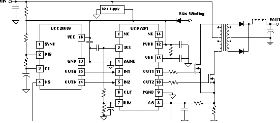 Figure 27. Intermediate Bus Converter
9.2.2.1 Design Requirements
In this design example, the input current is sensed by a current shunt, the cycle-by-cycle protection threshold is set at 5 A.
9.2.2.2 Detailed Design Procedure
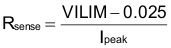
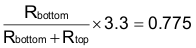
The current limit threshold can be set to any value between 0.25 V and 1.0 V, so Rsense need to be between 0.045 Ω and 0.195 Ω. Let’s choose Rsense as 0.15 Ω. VILIM need to be 0.775 V in order to protect input current at 5 A.
Since the controller is analog, it cannot program the VILIM, however, VILIM can be implemented by a voltage divider connect the pin 2 of UCD7201. Since the voltage on pin 2 is 3.3 V, so the voltage divider needs to be:
9.2.3 Application Curves
See Figure 26.