SLUS645F February 2005 – December 2014 UCD7201
PRODUCTION DATA.
- 1 Features
- 2 Applications
- 3 Description
- 4 Revision History
- 5 Description (Continued)
- 6 Pin Configuration and Functions
- 7 Specifications
- 8 Detailed Description
- 9 Applications and Implementation
- 10Power Supply Recommendations
- 11Layout
- 12Device and Documentation Support
- 13Mechanical, Packaging, and Orderable Information
パッケージ・オプション
メカニカル・データ(パッケージ|ピン)
- PWP|14
サーマルパッド・メカニカル・データ
- PWP|14
発注情報
7 Specifications
7.1 Absolute Maximum Ratings(1)(2)
| MIN | MAX | UNIT | |||
|---|---|---|---|---|---|
| VDD | Supply Voltage | 16 | V | ||
| IDD | Supply Current | Quiescent | 20 | mA | |
| Switching, TA = 25°C, , TJ = 125°C, VDD = 12 V | 200 | ||||
| VOUT | Output Gate Drive Voltage | OUT | –1 | PVDD | V |
| IOUT(sink) | Output Gate Drive Current | OUT | 4.0 | A | |
| IOUT(source) | –4.0 | ||||
| Analog Input | ISET, CS | –0.3 | 3.6 | V | |
| ILIM | –0.3 | 3.6 | |||
| Digital I/O’s | IN, CLF | –0.3 | 3.6 | ||
| Power Dissipation | TA = 25°C (PWP-14 package), TJ = 125°C | 2.67 | W | ||
| TJ | Junction Operating Temperature | UCD7201 | –55 | 150 | °C |
(1) Stresses beyond those listed under “absolute maximum ratings” may cause permanent damage to the device. These are stress ratings only, and functional operation of the device at these or any other conditions beyond those indicated under “recommended operating conditions” is not implied. Exposure to absolute-maximum-rated conditions for extended periods may affect device reliability.
(2) All voltages are with respect to GND. Currents are positive into, negative out of the specified terminal.
7.2 Handling Ratings
| MIN | MAX | UNIT | |||
|---|---|---|---|---|---|
| Tstg | Storage temperature range | –65 | 150 | °C | |
| V(ESD) | Electrostatic discharge | Human body model (HBM), per ANSI/ESDA/JEDEC JS-001, all pins(1) | 2000 | V | |
| Charged device model (CDM), per JEDEC specification JESD22-C101, all pins(2) | 500 | ||||
(1) JEDEC document JEP155 states that 500-V HBM allows safe manufacturing with a standard ESD control process.
(2) JEDEC document JEP157 states that 250-V CDM allows safe manufacturing with a standard ESD control process.
7.3 Recommended Operating Conditions
over operating free-air temperature range (unless otherwise noted)| MIN | TYP | MAX | UNIT | ||
|---|---|---|---|---|---|
| Supply Voltage, VDD | 4.25 | 12 | 14.5 | V | |
| Supply bypass capacitance | 1 | μF | |||
| Reference bypass capacitance | 0.22 | ||||
| Operating junction temperature | –40 | 105 | °C | ||
7.4 Thermal Information
| THERMAL METRIC(1) | UCD7201 | UNIT | |
|---|---|---|---|
| PWP | |||
| 14 PINS | |||
| RθJA | Junction-to-ambient thermal resistance | 50.7 | °C/W |
| RθJC(top) | Junction-to-case (top) thermal resistance | 31.8 | |
| RθJB | Junction-to-board thermal resistance | 27.8 | |
| ψJT | Junction-to-top characterization parameter | 1.2 | |
| ψJB | Junction-to-board characterization parameter | 27.6 | |
| RθJC(bot) | Junction-to-case (bottom) thermal resistance | 4.1 | |
(1) For more information about traditional and new thermal metrics, see the IC Package Thermal Metrics application report, SPRA953.
7.5 Electrical Characteristics
VDD = 12 V, 4.7-μF capacitor from VDD to GND, 0.22μF from 3V3 to AGND, TA = TJ = -40°C to 105°C, (unless otherwise noted).| PARAMETER | TEST CONDITIONS | MIN | TYP | MAX | UNIT | |
|---|---|---|---|---|---|---|
| SUPPLY SECTION | ||||||
| Supply current, OFF | VDD = 4.2 V | - | 200 | 400 | μA | |
| Supply current | Outputs not switching IN = LOW | - | 1.5 | 2.5 | mA | |
| LOW VOLTAGE UNDERVOLTAGE LOCKOUT | ||||||
| VDD UVLO ON | 4.25 | 4.5 | 4.75 | V | ||
| VDD UVLO OFF | 4.05 | 4.25 | 4.45 | |||
| VDD UVLO hysteresis | 150 | 250 | 350 | mV | ||
| REFERENCE / EXTERNAL BIAS SUPPLY | ||||||
| 3V3 initial set point | TA = 25°C, ILOAD = 0 | 3.267 | 3.3 | 3.333 | V | |
| 3V3 set point over temperature | 3.234 | 3.3 | 3.366 | |||
| 3V3 load regulation | ILOAD = 1 mA to 10 mA, VDD = 5 V | - | 1 | 6.6 | mV | |
| 3V3 line regulation | VDD = 4.75 V to 12 V, ILOAD = 10 mA | - | 1 | 6.6 | ||
| Short circuit current | VDD = 4.75 to 12 V | 11 | 20 | 35 | mA | |
| 3V3 OK threshold, ON | 3.3 V rising | 2.9 | 3.0 | 3.1 | V | |
| 3V3 OK threshold, OFF | 3.3 V falling | 2.7 | 2.8 | 2.9 | ||
| INPUT SIGNAL | ||||||
| HIGH, positive-going input threshold voltage (VIT+) | 1.65 | - | 2.08 | V | ||
| LOW negative-going input threshold voltage (VIT-) | 1.16 | - | 1.5 | |||
| Input voltage hysteresis, (VIT+ - VIT-) | 0.6 | - | 0.8 | |||
| Frequency | - | - | 2 | MHz | ||
| CURRENT LIMIT (ILIM) | ||||||
| ILIM internal current limit threshold | ILIM = OPEN | 0.51 | 0.55 | 0.58 | V | |
| ILIM maximum current limit threshold | ILIM = 3.3 V | 1.05 | 1.10 | 1.15 | ||
| ILIM current limit threshold | ILIM = 0.75 V | 0.700 | 0.725 | 0.750 | ||
| ILIM minimum current limit threshold | ILIM = 0.25 V | 0.21 | 0.23 | 0.25 | ||
| CLF output high level | CS > ILIM , ILOAD = -7 mA | 2.64 | - | - | ||
| CLF output low level | CS ≤ ILIM, ILOAD = 7 mA | - | - | 0.66 | ||
| Propagation delay from IN to CLF | IN rising to CLF falling after a current limit event | - | 10 | 20 | ns | |
| CURRENT SENSE COMPARATOR | ||||||
| Bias voltage | Includes CS comp offset | 5 | 25 | 50 | mV | |
| Input bias current | - | –1 | - | μA | ||
| Propagation delay from CS to OUTx | ILIM = 0.5 V, measured on OUTx, CS = threshold + 60 mV | - | 25 | 40 | ns | |
| Propagation delay from CS to CLF | ILIM = 0.5 V, measured on CLF, CS = threshold + 60 mV | - | 25 | 50 | ||
| CURRENT SENSE DISCHARGE TRANSISTOR | ||||||
| Discharge resistance | IN = low, resistance from CS to AGND | 10 | 35 | 75 | Ω | |
| OUTPUT DRIVERS | ||||||
| Source current | VDD = 12 V, IN = high, OUTx = 5 V | 4 | A | |||
| Sink current | VDD = 12 V, IN = low, OUTx = 5 V | 4 | ||||
| Source current | VDD = 4.75 V, IN = high, OUTx = 0 | 2 | ||||
| Sink current | VDD = 4.75 V, IN = low, OUTx = 4.75 V | 3 | ||||
| Rise time, tR | CLOAD= 2.2 nF, VDD = 12 V | 10 | 20 | ns | ||
| Fall time, tF | CLOAD = 2.2 nF, VDD = 12 V | 10 | 15 | |||
| Output with VDD < UVLO | VDD =1.0 V, ISINK = 10 mA | 0.8 | 1.2 | V | ||
| Propagation delay from IN to OUT1, tD1 | CLOAD = 2.2 nF, VDD = 12 V, CLK rising | 20 | 35 | ns | ||
| Propagation delay from IN to OUT2, tD2 | CLOAD = 2.2 nF, VDD = 12 V, CLK falling | 20 | 35 | |||
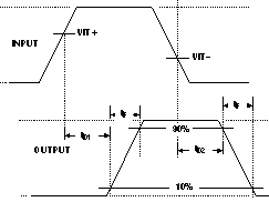 Figure 1. Timing Diagram
7.6 Typical Characteristics
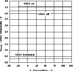 Figure 2. UVLO Thresholds vs Temperature
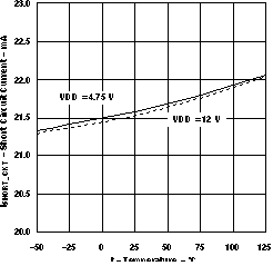 Figure 4. 3V3 Short Circuit Current vs Temperature
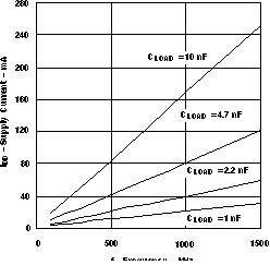 Figure 6. Supply Current vs Frequency (VDD = 8 V)
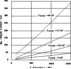 Figure 8. Supply Current vs Frequency (VDD = 12V)
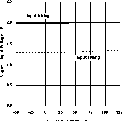 Figure 10. Input Thresholds vs Temperature
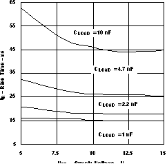 Figure 12. Rise Time vs Supply Voltage
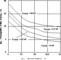 Figure 14. IN to OUTx Propagation Delay Rising vs Supply Voltage
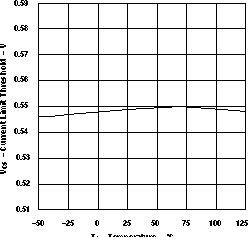 Figure 16. Default Current Limit Threshold vs Temperature
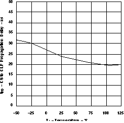 Figure 18. CS to CLF Propagation Delay vs Temperature
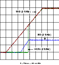 Figure 20. Start-Up Behavior at VDD = 12 V (Input Tied to 3V3)
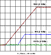 Figure 22. Start-Up Behavior at VDD = 12 V (Input Shortened to GND)
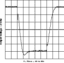 Figure 24. Output Rise and Fall Time (VDD = 12 V, CLOAD = 10 nF)
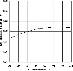 Figure 3. 3V3 Reference Voltage vs Temperature
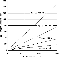 Figure 5. Supply Current vs Frequency (VDD = 5 V)
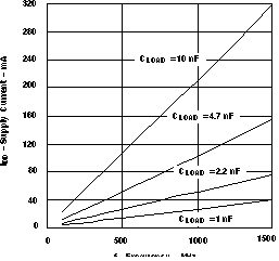 Figure 7. Supply Current vs Frequency (VDD = 10 V)
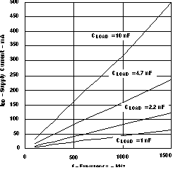 Figure 9. Supply Current vs Frequency (VDD = 15 V)
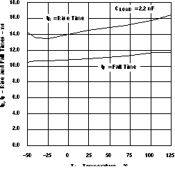 Figure 11. Output Rise Time and Fall Time vs Temperature (VDD = 12 V)
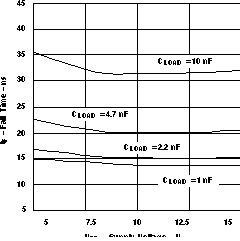 Figure 13. Fall Time vs Supply Voltage
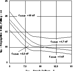 Figure 15. IN to OUTx Propagation Delay Falling vs Supply Voltage
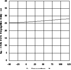 Figure 17. CS to OUTx Propagation Delay vs Temperature
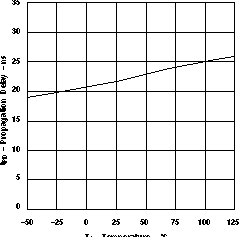 Figure 19. IN to OUT Propagation Delay vs Temperature
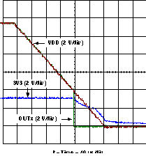 Figure 21. Shut Down Behavior at VDD = 12 V (Input Tied to 3V3)
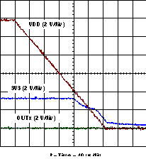 Figure 23. Shut Down Behavior at VDD = 12 V (Input Shortened to GND)