JAJSHD6B August 2016 – May 2019 UCD90320
PRODUCTION DATA.
- 1 特長
- 2 アプリケーション
- 3 概要
- 4 改訂履歴
- 5 概要(続き)
- 6 Pin Configuration and Functions
- 7 Specifications
-
8 Detailed Description
- 8.1 Overview
- 8.2 Functional Block Diagram
- 8.3 Feature Description
- 8.4
Device Functional Modes
- 8.4.1 Rail Monitoring Configuration
- 8.4.2 GPI Configuration
- 8.4.3 Rail Sequence Configuration
- 8.4.4 Fault Responses Configuration
- 8.4.5 GPO Configuration
- 8.4.6 Margining Configuration
- 8.4.7 Pin Selected Rail States Configuration
- 8.4.8 Watchdog Timer
- 8.4.9 System Reset Function
- 8.4.10 Cascading Multiple Devices
- 8.4.11 Rail Monitoring
- 8.4.12 Status Monitoring
- 8.4.13 Data and Error Logging to EEPROM Memory
- 8.4.14 Black Box First Fault Logging
- 8.4.15 PMBus Address Selection
- 8.4.16 ADC Reference
- 8.4.17 Device Reset
- 8.4.18 Brownout
- 8.4.19 Internal Fault Management
- 8.5 Device Configuration and Programming
- 9 Application and Implementation
- 10Power Supply Recommendations
- 11Layout
- 12デバイスおよびドキュメントのサポート
- 13メカニカル、パッケージ、および注文情報
8.4.14 Black Box First Fault Logging
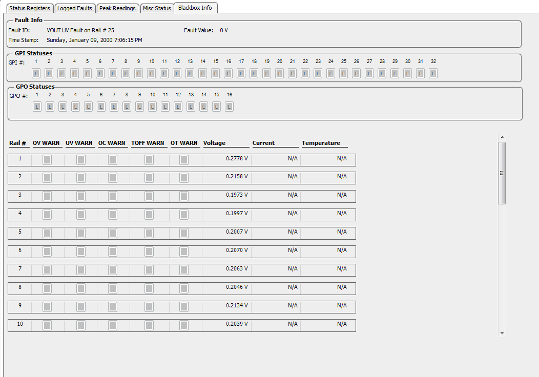
The first fault in a system failure event is usually critical to diagnose the root cause. An innovative Black Box Fault Logging feature is introduced in UCD90320 to accelerate the debugging process. When UCD90320 detects the first fault, the device records and saves the status of each rail and I/O pin in a special area of the EEPROM reserved for this function. The device does not save the subsequent faults and monitoring statuses into the Black Box Fault Log, but instead records them into the standard fault log. The Black Box Fault Log must be cleared in order to acknowledge the next fault.
 Figure 34. Black Box Fault Logging Window (Status ►Blackbox Info tab)