JAJSHD6B August 2016 – May 2019 UCD90320
PRODUCTION DATA.
- 1 特長
- 2 アプリケーション
- 3 概要
- 4 改訂履歴
- 5 概要(続き)
- 6 Pin Configuration and Functions
- 7 Specifications
-
8 Detailed Description
- 8.1 Overview
- 8.2 Functional Block Diagram
- 8.3 Feature Description
- 8.4
Device Functional Modes
- 8.4.1 Rail Monitoring Configuration
- 8.4.2 GPI Configuration
- 8.4.3 Rail Sequence Configuration
- 8.4.4 Fault Responses Configuration
- 8.4.5 GPO Configuration
- 8.4.6 Margining Configuration
- 8.4.7 Pin Selected Rail States Configuration
- 8.4.8 Watchdog Timer
- 8.4.9 System Reset Function
- 8.4.10 Cascading Multiple Devices
- 8.4.11 Rail Monitoring
- 8.4.12 Status Monitoring
- 8.4.13 Data and Error Logging to EEPROM Memory
- 8.4.14 Black Box First Fault Logging
- 8.4.15 PMBus Address Selection
- 8.4.16 ADC Reference
- 8.4.17 Device Reset
- 8.4.18 Brownout
- 8.4.19 Internal Fault Management
- 8.5 Device Configuration and Programming
- 9 Application and Implementation
- 10Power Supply Recommendations
- 11Layout
- 12デバイスおよびドキュメントのサポート
- 13メカニカル、パッケージ、および注文情報
8.4.16 ADC Reference
Using the V33A pin as ADC reference voltage by default provides a cost-effective solution. However, internal voltage reference has a higher Total Unadjusted Error. Also, voltage variations on the V33A pin affect ADC readings, such as when the device is powered down. In order to achieve better ADC accuracy, an external voltage reference can be connected to the VREFA+ and VREFA- pins. Ensure that the external reference voltage stays in regulation whenever V33D is above VBOR threshold. This limitation allows accurate ADC readings in full V33D operating range.
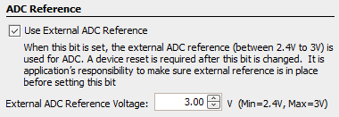
The external reference voltage level must be configured into the Fusion Digital Power Designer software to give correct ADC readings.
 Figure 35. ADC Reference Configuration Window (Global Configuration ► Misc Config)