SLRS060C May 2012 – November 2016 ULN2003V12
PRODUCTION DATA.
- 1 Features
- 2 Applications
- 3 Description
- 4 Revision History
- 5 Pin Configuration and Functions
- 6 Specifications
- 7 Detailed Description
- 8 Applications and Implementation
- 9 Power Supply Recommendations
- 10Layout
- 11Device and Documentation Support
- 12Mechanical, Packaging, and Orderable Information
パッケージ・オプション
メカニカル・データ(パッケージ|ピン)
サーマルパッド・メカニカル・データ
発注情報
8 Applications and Implementation
NOTE
Information in the following applications sections is not part of the TI component specification, and TI does not warrant its accuracy or completeness. TI’s customers are responsible for determining suitability of components for their purposes. Customers should validate and test their design implementation to confirm system functionality.
8.1 Application Information
Peripheral drivers such as the ULN2003V12 are primarily used in the following applications:
- Stepper Motor Driving
- Relay and Solenoid Driving
- LED Driving
- Logic Level Shifting
Peripheral Drivers are not limited to one specific application at a time, but can be used for all of these applications simultaneously. For example, one device could enable driving one stepper motor, driving one relay, driving an LED, and shifting a 3.3-V logic signal to a 12-V logic signal at the same time.
8.2 Typical Applications
8.2.1 Unipolar Stepper Motor Driver
The Figure 4 shows an implementation of ULN2003V12 for driving a unipolar stepper motor.
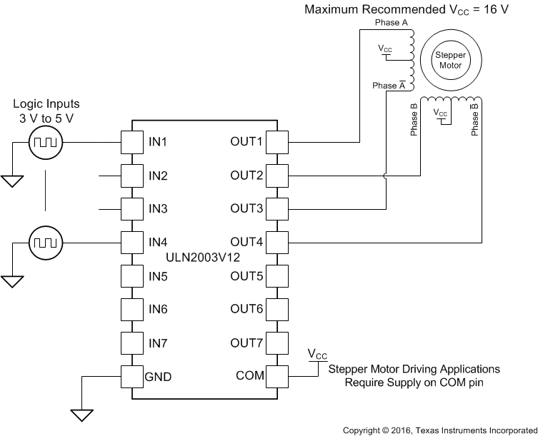 Figure 4. ULN2003V12 as a Stepper Motor Driver
8.2.1.1 Design Requirements
The unconnected input channels can be used for other functions. When an input pin is left open, the internal 300-kΩ pulldown resistor pulls the respective input pin to GND potential. For higher noise immunity use an external short across an unconnected input and GND pins. See Stepper Motor Driving with Peripheral Drivers (SLVA767) for additional information regarding stepper motor driving.
8.2.1.2 Application Curves
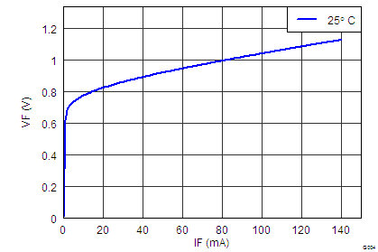 Figure 5. Freewheeling Diode VF vs IF
8.2.2 Inverting Logic Level Shifter
To use ULN2003V12 as an open-drain inverting logic level shifter, configure the device as shown in Figure 6. The device input and output logic levels can also be set independently. When using different channel input and output logic voltages, connect the ULN2003V12 COM pin to the maximum voltage.
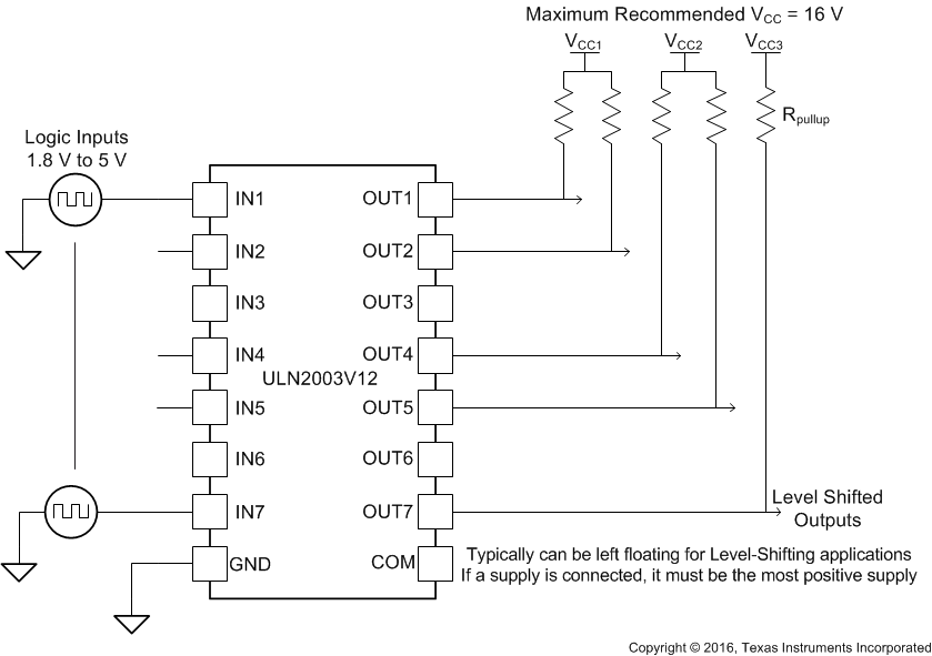 Figure 6. ULN2003V12 as Inverting Logic Level Shifter
8.2.2.1 Design Requirements
ULN2003V12 can be used in digital applications requiring logic level shifting up to 16 V at the output side. Because the device pulls the output transistor low when input is high, this configuration is useful for applications requiring inverting logic with the level shifting operation.
8.2.2.2 Detailed Design Procedure
To operate in level shifting operation, timing and propagation delay must be kept in mind. Depending on the pullup resistors at the output ULN2003V12 exhibits different propagation delays. The choice of pullup resistor is dependent on the drive required at the output. The device can pull output to ground with the output transistor, but to transition from low to high output resistor plays a critical role. If high drive at output is required, use Equation 1 to calculate a lower resistance.
For example, a drive of 5 mA is required at the output for 1.8-V to 5-V translation application.
8.2.3 Maximum Supply Selector
The Figure 7 implements a maximum supply selector along with a 4-channel logic level shifter using a single ULN20003V12.
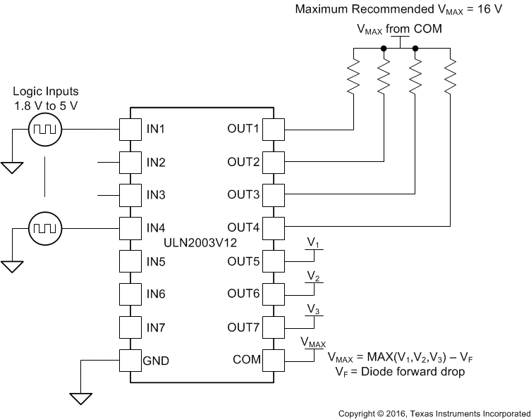 Figure 7. ULN2003V12 as a Maximum Supply Selector
8.2.3.1 Design Requirements
This setup configures ULN2003V12’s channel clamp diodes OUT5 to OUT7 in a diode-OR configuration and thus the maximum supply among V1, V2, and V3 becomes available at the COM pin. The maximum supply is then used as a pullup voltage for level shifters. Limit the net GND pin current to less than 100-mA DC to ensure reliability of the conducting diode. The unconnected inputs IN5 to IN7 are pulled to GND potential through
300-kΩ internal pulldown resistor.
8.2.4 Constant Current LED Driver
When configured as per Figure 8, the ULN2003V12 outputs OUT1 to OUT6 act as independent constant current sources.
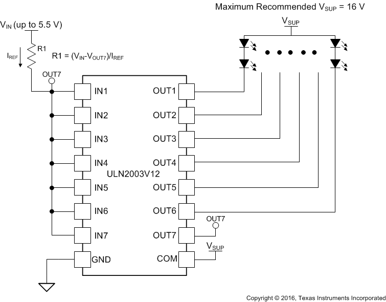 Figure 8. ULN2003V12 as a Constant Current Driver
8.2.4.1 Design Requirements
The current flowing through the resistor R1 is mirrored on all other channels. To increase the current sourcing connect several output channels in parallel. To ensure best current mirroring, set voltage drop across connected load such that VOUTx matches VOUT7.
8.2.5 NOR Logic Driver
Figure 9 shows a NOR Logic driver implementation using the ULN2003V12 device.
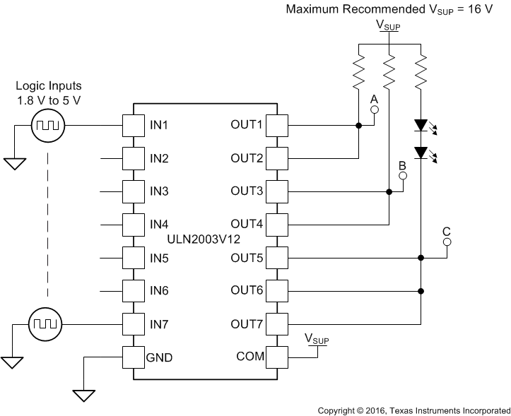 Figure 9. ULN2003V12 as a NOR driver
8.2.5.1 Design Requirements
The output channels sharing a common pullup resistor implement a logic NOR of the respective channel inputs. Node A is controlled by inputs IN1 and IN2 as described in Table 2 (Positive Logic Function: A = IN1+IN2). Node B is controlled by inputs IN3 and IN4 as described in Table 3 (Positive Logic Function: B = IN3+IN4). Node C is controlled by inputs IN5, IN6, and IN7 as described in Table 4 (Positive Logic Function C = IN5+IN6+IN7).
Table 2. Output A Function Table
| IN1 | IN2 | A |
|---|---|---|
| L | L | H |
| X | H | L |
| H | X | L |
Table 3. Output B Function Table
| IN3 | IN4 | B |
|---|---|---|
| L | L | H |
| X | H | L |
| H | X | L |
Table 4. Output C Function Table
| IN5 | IN6 | IN7 | C | LED |
|---|---|---|---|---|
| L | L | L | H | OFF |
| X | X | H | L | ON |
| X | H | X | L | ON |
| H | X | X | L | ON |