SLRS060C May 2012 – November 2016 ULN2003V12
PRODUCTION DATA.
- 1 Features
- 2 Applications
- 3 Description
- 4 Revision History
- 5 Pin Configuration and Functions
- 6 Specifications
- 7 Detailed Description
- 8 Applications and Implementation
- 9 Power Supply Recommendations
- 10Layout
- 11Device and Documentation Support
- 12Mechanical, Packaging, and Orderable Information
パッケージ・オプション
メカニカル・データ(パッケージ|ピン)
サーマルパッド・メカニカル・データ
発注情報
6 Specifications
6.1 Absolute Maximum Ratings
Specified at TJ = –40°C to 125°C (unless otherwise noted)(1)| MIN | MAX | UNIT | ||
|---|---|---|---|---|
| Pins IN1 – IN7 to GND voltage, VIN | –0.3 | 5.5 | V | |
| Pins OUT1 – OUT7 to GND voltage, VOUT | 20 | V | ||
| Pin COM to GND voltage, VCOM | 20 | V | ||
| Maximum GND-pin continuous current, IGND | 100ºC < TJ < 125°C | 700 | mA | |
| TJ < 100°C | 1 | A | ||
| Operating virtual junction temperature, TJ | –55 | 150 | °C | |
| Storage temperature, Tstg | –55 | 150 | °C | |
(1) Stresses beyond those listed under Absolute Maximum Ratings may cause permanent damage to the device. These are stress ratings only, which do not imply functional operation of the device at these or any other conditions beyond those indicated under Recommended Operating Conditions. Exposure to absolute-maximum-rated conditions for extended periods may affect device reliability.
6.2 ESD Ratings
| VALUE | UNIT | |||
|---|---|---|---|---|
| V(ESD) | Electrostatic discharge | Human-body model (HBM), per ANSI/ESDA/JEDEC JS-001(1) | ±2000 | V |
| Charged-device model (CDM), per JEDEC specification JESD22-C101(2) | ±500 | |||
(1) JEDEC document JEP155 states that 500-V HBM allows safe manufacturing with a standard ESD control process.
(2) JEDEC document JEP157 states that 250-V CDM allows safe manufacturing with a standard ESD control process.
6.3 Recommended Operating Conditions
over operating free-air temperature range (unless otherwise noted)| MIN | MAX | UNIT | |||
|---|---|---|---|---|---|
| VOUT | Channel off-state output pullup voltage | 16 | V | ||
| VCOM | COM pin voltage | 16 | V | ||
| IOUT(ON)(1) | Per channel continuous sink current | VINx = 3.3 V | 100(1) | mA | |
| VINx = 5 V | 140(1) | ||||
| TJ | Operating junction temperature | –40 | 125 | ºC | |
(1) See Absolute Maximum Ratings for TJ dependent absolute maximum GND-pin current.
6.4 Thermal Information
| THERMAL METRIC(1) | ULN2003V12 | UNIT | ||
|---|---|---|---|---|
| D (SOIC) | PW (TSSOP) | |||
| 16 PINS | 16 PINS | |||
| RθJA | Junction-to-ambient thermal resistance | 104.8 | 130.6 | °C/W |
| RθJC(top) | Junction-to-case (top) thermal resistance | 63.7 | 62.7 | °C/W |
| RθJB | Junction-to-board thermal resistance | 62.3 | 76.1 | °C/W |
| ψJT | Junction-to-top characterization parameter | 27.1 | 15.9 | °C/W |
| ψJB | Junction-to-board characterization parameter | 62.1 | 75.5 | °C/W |
(1) For more information about traditional and new thermal metrics, see the Semiconductor and IC Package Thermal Metrics application report.
6.5 Electrical Characteristics
Typical values are at TJ = 25°C, minimum and maximum values over the recommended junction temperature rangeTJ = –40°C to 125°C, and over recommended operating conditions (unless otherwise noted)
| PARAMETER | TEST CONDITIONS | MIN | TYP | MAX | UNIT | |
|---|---|---|---|---|---|---|
| INPUTS IN1 THROUGH IN7 PARAMETERS | ||||||
| VI(ON) | IN1–IN7 logic high input voltage | Vpullup = 3.3 V, Rpullup = 1 kΩ, IOUTX = 3.2 mA | 1.65 | V | ||
| VI(OFF) | IN1–IN7 logic low input voltage | Vpullup = 3.3 V, Rpullup = 1 kΩ, IOUTX < 20 µA | 0.6 | |||
| II(ON) | IN1–IN7 ON state input current | Vpullup = 12 V, VINx = 3.3 V | 12 | 25 | µA | |
| II(OFF) | IN1–IN7 OFF state input leakage | Vpullup = 12 V, VINx = 0 V | 250 | nA | ||
| OUTPUTS OUT1 THROUGH OUT7 PARAMETERS | ||||||
| VOL(VCE-SAT) | OUT1–OUT7 low-level output voltage | VINX = 3.3 V, IOUTX = 20 mA | 0.12 | 0.15 | V | |
| VINX = 3.3 V, IOUTX = 100 mA | 0.6 | 0.75 | ||||
| VINX = 5 V, IOUTX = 20 mA | 0.09 | 0.11 | ||||
| VINX = 5 V, IOUTX = 140 mA | 0.6 | 0.75 | ||||
| IOUT(ON) | OUT1–OUT7 ON-state continuous current at VOUTX = 0.6 V(1)(2) | VINX = 3.3 V, VOUTX = 0.6 V | 80 | 100 | mA | |
| VINX = 5 V, VOUTX = 0.6 V | 95 | 140 | ||||
| IOUT(OFF)(ICEX) | OUT1–OUT7 OFF-state leakage current | VINX = 0 V, VOUTX = VCOM = 16 V | 0.5 | µA | ||
| SWITCHING PARAMETERS(3)(5) | ||||||
| tPHL | OUT1–OUT7 logic high propagation delay | VINX = 3.3 V, Vpullup = 12 V, Rpullup = 1 kΩ | 50 | 70 | ns | |
| tPLH | OUT1–OUT7 logic low propagation delay | VINX = 3.3V, Vpullup = 12 V, Rpullup = 1 kΩ | 121 | 140 | ns | |
| t CHANNEL | Channel-to-channel delay | Over recommended operating conditions and with same test conditions on channels. | 15 | 50 | ns | |
| RPD | IN1–IN7 input pulldown resistance | 210 | 300 | 390 | kΩ | |
| ζ | IN1–IN7 input filter time constant | 9 | ns | |||
| COUT | OUT1–OUT7 output capacitance | VINX = 3.3 V, VOUTX = 0.4 V | 15 | pF | ||
| FREE-WHEELING DIODE PARAMETERS(5)(4) | ||||||
| VF | Forward voltage drop | IF-peak = 140 mA, VF = VOUTx – VCOM | 1.2 | V | ||
| IF-peak | Diode peak forward current | 140 | mA | |||
(1) The typical continuous current rating is limited by VOL= 0.6 V. Whereas, absolute maximum operating continuous current may be limited by the Thermal performance parameters listed in the Thermal Information and other reliability parameters listed in Recommended Operating Conditions.
(2) See Absolute Maximum Ratings for TJ dependent absolute maximum GND-pin current.
(3) Rise and fall propagation delays, tPHL and tPLH, are measured between 50% values of the input and the corresponding output signal amplitude transition.
(4) Not rated for continuous current operation. For higher reliability, use an external freewheeling diode for inductive loads resulting in more than specified maximum free-wheeling. Diode peak current across various temperature conditions.
(5) Specified by design only. Validated during qualification. Not measured in production testing.
6.6 Typical Characteristics
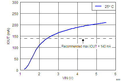
TA = 25ºC Figure 1. Load Current, 1-Channel at VOL = 0.6 V
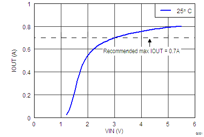
 Figure 2. Load Current, 7-Channels in Parallel at VOL = 0.6 V