JAJSHP9E November 2007 – July 2019 VCA824
PRODUCTION DATA.
- 1 特長
- 2 アプリケーション
- 3 概要
- 4 改訂履歴
- 5 Device Comparison Table
- 6 Pin Configuration and Functions
-
7 Specifications
- 7.1 Absolute Maximum Ratings
- 7.2 ESD Ratings
- 7.3 Recommended Operating Conditions
- 7.4 Thermal Information
- 7.5 Electrical Characteristics: VS = ±5 V
- 7.6 Typical Characteristics: VS = ±5 V, AVMAX = 2 V/V
- 7.7 Typical Characteristics: VS = ±5 V, AVMAX = 10 V/V
- 7.8 Typical Characteristics: VS = ±5 V, AVMAX = 40 V/V
- 8 Detailed Description
- 9 Application and Implementation
- 10Power Supply Recommendations
- 11Layout
- 12デバイスおよびドキュメントのサポート
- 13メカニカル、パッケージ、および注文情報
パッケージ・オプション
メカニカル・データ(パッケージ|ピン)
サーマルパッド・メカニカル・データ
- D|14
発注情報
8.4.8 Input and ESD Protection
The VCA824 is built using a very high-speed complementary bipolar process. The internal junction breakdown voltages are relatively low for these very small geometry devices. These breakdowns are reflected in the Absolute Maximum Ratings.
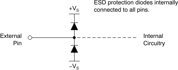
All pins on the VCA824 are internally protected from ESD by means of a pair of back-to-back reverse-biased diodes to either power supply, as shown in Figure 64. These diodes begin to conduct when the pin voltage exceeds either power supply by about 0.7 V. This situation can occur with loss of the amplifier power supplies while a signal source is still present. The diodes can typically withstand a continuous current of 30 mA without destruction. To ensure long-term reliability, however, diode current should be externally limited to 10 mA whenever possible.
 Figure 64. Internal ESD Protection