JAJSDF5A June 2017 – April 2020 ADC12DJ3200
PRODUCTION DATA.
- 1 特長
- 2 アプリケーション
- 3 概要
- 4 改訂履歴
- 5 概要(続き)
- 6 Pin Configuration and Functions
-
7 Specifications
- 7.1 Absolute Maximum Ratings
- 7.2 ESD Ratings
- 7.3 Recommended Operating Conditions
- 7.4 Thermal Information
- 7.5 Electrical Characteristics - DC Specifications
- 7.6 Electrical Characteristics - Power Consumption
- 7.7 Electrical Characteristics: AC Specifications (Dual-Channel Mode)
- 7.8 Electrical Characteristics: AC Specifications (Single-Channel Mode)
- 7.9 Timing Requirements
- 7.10 Switching Characteristics
- 7.11 Typical Characteristics
-
8 Detailed Description
- 8.1 Overview
- 8.2 Functional Block Diagram
- 8.3
Feature Description
- 8.3.1 Device Comparison
- 8.3.2 Analog Inputs
- 8.3.3 ADC Core
- 8.3.4 Temperature Monitoring Diode
- 8.3.5 Timestamp
- 8.3.6 Clocking
- 8.3.7 Digital Down Converters (Dual-Channel Mode Only)
- 8.3.8 JESD204B Interface
- 8.3.9 Alarm Monitoring
- 8.4
Device Functional Modes
- 8.4.1 Dual-Channel Mode
- 8.4.2 Single-Channel Mode (DES Mode)
- 8.4.3 JESD204B Modes
- 8.4.4 Power-Down Modes
- 8.4.5 Test Modes
- 8.4.6 Calibration Modes and Trimming
- 8.4.7 Offset Calibration
- 8.4.8 Trimming
- 8.4.9 Offset Filtering
- 8.5 Programming
- 8.6
Register Maps
- 8.6.1 Memory Map
- 8.6.2
Register Descriptions
- 8.6.2.1
Standard SPI-3.0 (0x000 to 0x00F)
- Table 46. Standard SPI-3.0 Registers
- 8.6.2.1.1 Configuration A Register (address = 0x000) [reset = 0x30]
- 8.6.2.1.2 Device Configuration Register (address = 0x002) [reset = 0x00]
- 8.6.2.1.3 Chip Type Register (address = 0x003) [reset = 0x03]
- 8.6.2.1.4 Chip ID Register (address = 0x004 to 0x005) [reset = 0x0020]
- 8.6.2.1.5 Chip Version Register (address = 0x006) [reset = 0x01]
- 8.6.2.1.6 Vendor Identification Register (address = 0x00C to 0x00D) [reset = 0x0451]
- 8.6.2.2 User SPI Configuration (0x010 to 0x01F)
- 8.6.2.3
Miscellaneous Analog Registers (0x020 to 0x047)
- 8.6.2.3.1 Clock Control Register 0 (address = 0x029) [reset = 0x00]
- 8.6.2.3.2 Clock Control Register 1 (address = 0x02A) [reset = 0x00]
- 8.6.2.3.3 SYSREF Capture Position Register (address = 0x02C-0x02E) [reset = Undefined]
- 8.6.2.3.4 INA Full-Scale Range Adjust Register (address = 0x030-0x031) [reset = 0xA000]
- 8.6.2.3.5 INB Full-Scale Range Adjust Register (address = 0x032-0x033) [reset = 0xA000]
- 8.6.2.3.6 Internal Reference Bypass Register (address = 0x038) [reset = 0x00]
- 8.6.2.3.7 TMSTP± Control Register (address = 0x03B) [reset = 0x00]
- 8.6.2.4 Serializer Registers (0x048 to 0x05F)
- 8.6.2.5
Calibration Registers (0x060 to 0x0FF)
- 8.6.2.5.1 Input Mux Control Register (address = 0x060) [reset = 0x01]
- 8.6.2.5.2 Calibration Enable Register (address = 0x061) [reset = 0x01]
- 8.6.2.5.3 Calibration Configuration 0 Register (address = 0x062) [reset = 0x01]
- 8.6.2.5.4 Calibration Status Register (address = 0x06A) [reset = Undefined]
- 8.6.2.5.5 Calibration Pin Configuration Register (address = 0x06B) [reset = 0x00]
- 8.6.2.5.6 Calibration Software Trigger Register (address = 0x06C) [reset = 0x01]
- 8.6.2.5.7 Low-Power Background Calibration Register (address = 0x06E) [reset = 0x88]
- 8.6.2.5.8 Calibration Data Enable Register (address = 0x070) [reset = 0x00]
- 8.6.2.5.9 Calibration Data Register (address = 0x071) [reset = Undefined]
- 8.6.2.5.10 Channel A Gain Trim Register (address = 0x07A) [reset = Undefined]
- 8.6.2.5.11 Channel B Gain Trim Register (address = 0x07B) [reset = Undefined]
- 8.6.2.5.12 Band-Gap Reference Trim Register (address = 0x07C) [reset = Undefined]
- 8.6.2.5.13 VINA Input Resistor Trim Register (address = 0x07E) [reset = Undefined]
- 8.6.2.5.14 VINB Input Resistor Trim Register (address = 0x07F) [reset = Undefined]
- 8.6.2.5.15 Timing Adjust for A-ADC, Single-Channel Mode, Foreground Calibration Register (address = 0x080) [reset = Undefined]
- 8.6.2.5.16 Timing Adjust for B-ADC, Single-Channel Mode, Foreground Calibration Register (address = 0x081) [reset = Undefined]
- 8.6.2.5.17 Timing Adjust for A-ADC, Single-Channel Mode, Background Calibration Register (address = 0x082) [reset = Undefined]
- 8.6.2.5.18 Timing Adjust for C-ADC, Single-Channel Mode, Background Calibration Register (address = 0x083) [reset = Undefined]
- 8.6.2.5.19 Timing Adjust for C-ADC, Single-Channel Mode, Background Calibration Register (address = 0x084) [reset = Undefined]
- 8.6.2.5.20 Timing Adjust for B-ADC, Single-Channel Mode, Background Calibration Register (address = 0x085) [reset = Undefined]
- 8.6.2.5.21 Timing Adjust for A-ADC, Dual-Channel Mode Register (address = 0x086) [reset = Undefined]
- 8.6.2.5.22 Timing Adjust for C-ADC Acting for A-ADC, Dual-Channel Mode Register (address = 0x087) [reset = Undefined]
- 8.6.2.5.23 Timing Adjust for C-ADC Acting for B-ADC, Dual-Channel Mode Register (address = 0x088) [reset = Undefined]
- 8.6.2.5.24 Timing Adjust for B-ADC, Dual-Channel Mode Register (address = 0x089) [reset = Undefined]
- 8.6.2.5.25 Offset Adjustment for A-ADC and INA Register (address = 0x08A-0x08B) [reset = Undefined]
- 8.6.2.5.26 Offset Adjustment for A-ADC and INB Register (address = 0x08C-0x08D) [reset = Undefined]
- 8.6.2.5.27 Offset Adjustment for C-ADC and INA Register (address = 0x08E-0x08F) [reset = Undefined]
- 8.6.2.5.28 Offset Adjustment for C-ADC and INB Register (address = 0x090-0x091) [reset = Undefined]
- 8.6.2.5.29 Offset Adjustment for B-ADC and INA Register (address = 0x092-0x093) [reset = Undefined]
- 8.6.2.5.30 Offset Adjustment for B-ADC and INB Register (address = 0x094-0x095) [reset = Undefined]
- 8.6.2.5.31 Offset Filtering Control 0 Register (address = 0x097) [reset = 0x00]
- 8.6.2.5.32 Offset Filtering Control 1 Register (address = 0x098) [reset = 0x33]
- 8.6.2.6
ADC Bank Registers (0x100 to 0x15F)
- 8.6.2.6.1 Timing Adjustment for Bank 0 (0° Clock) Register (address = 0x102) [reset = Undefined]
- 8.6.2.6.2 Timing Adjustment for Bank 0 (–90° Clock) Register (address = 0x103) [reset = Undefined]
- 8.6.2.6.3 Timing Adjustment for Bank 1 (0° Clock) Register (address = 0x112) [reset = Undefined]
- 8.6.2.6.4 Timing Adjustment for Bank 1 (–90° Clock) Register (address = 0x113) [reset = Undefined]
- 8.6.2.6.5 Timing Adjustment for Bank 2 (0° Clock) Register (address = 0x122) [reset = Undefined]
- 8.6.2.6.6 Timing Adjustment for Bank 2 (–90° Clock) Register (address = 0x123) [reset = Undefined]
- 8.6.2.6.7 Timing Adjustment for Bank 3 (0° Clock) Register (address = 0x132) [reset = Undefined]
- 8.6.2.6.8 Timing Adjustment for Bank 3 (–90° Clock) Register (address = 0x133) [reset = Undefined]
- 8.6.2.6.9 Timing Adjustment for Bank 4 (0° Clock) Register (address = 0x142) [reset = Undefined]
- 8.6.2.6.10 Timing Adjustment for Bank 4 (–90° Clock) Register (address = 0x143) [reset = Undefined]
- 8.6.2.6.11 Timing Adjustment for Bank 5 (0° Clock) Register (address = 0x152) [reset = Undefined]
- 8.6.2.6.12 Timing Adjustment for Bank 5 (–90° Clock) Register (address = 0x153) [reset = Undefined]
- 8.6.2.7 LSB Control Registers (0x160 to 0x1FF)
- 8.6.2.8
JESD204B Registers (0x200 to 0x20F)
- 8.6.2.8.1 JESD204B Enable Register (address = 0x200) [reset = 0x01]
- 8.6.2.8.2 JESD204B Mode Register (address = 0x201) [reset = 0x02]
- 8.6.2.8.3 JESD204B K Parameter Register (address = 0x202) [reset = 0x1F]
- 8.6.2.8.4 JESD204B Manual SYNC Request Register (address = 0x203) [reset = 0x01]
- 8.6.2.8.5 JESD204B Control Register (address = 0x204) [reset = 0x02]
- 8.6.2.8.6 JESD204B Test Pattern Control Register (address = 0x205) [reset = 0x00]
- 8.6.2.8.7 JESD204B DID Parameter Register (address = 0x206) [reset = 0x00]
- 8.6.2.8.8 JESD204B Frame Character Register (address = 0x207) [reset = 0x00]
- 8.6.2.8.9 JESD204B, System Status Register (address = 0x208) [reset = Undefined]
- 8.6.2.8.10 JESD204B Channel Power-Down Register (address = 0x209) [reset = 0x00]
- 8.6.2.8.11 JESD204B Extra Lane Enable (Link A) Register (address = 0x20A) [reset = 0x00]
- 8.6.2.8.12 JESD204B Extra Lane Enable (Link B) Register (address = 0x20B) [reset = 0x00]
- 8.6.2.9
Digital Down Converter Registers (0x210-0x2AF)
- 8.6.2.9.1 DDC Configuration Register (address = 0x210) [reset = 0x00]
- 8.6.2.9.2 Overrange Threshold 0 Register (address = 0x211) [reset = 0xF2]
- 8.6.2.9.3 Overrange Threshold 1 Register (address = 0x212) [reset = 0xAB]
- 8.6.2.9.4 Overrange Configuration Register (address = 0x213) [reset = 0x07]
- 8.6.2.9.5 DDC Configuration Preset Mode Register (address = 0x214) [reset = 0x00]
- 8.6.2.9.6 DDC Configuration Preset Select Register (address = 0x215) [reset = 0x00]
- 8.6.2.9.7 Digital Channel Binding Register (address = 0x216) [reset = 0x02]
- 8.6.2.9.8 Rational NCO Reference Divisor Register (address = 0x217 to 0x218) [reset = 0x0000]
- 8.6.2.9.9 NCO Synchronization Register (address = 0x219) [reset = 0x02]
- 8.6.2.9.10 NCO Frequency (DDC A or DDC B and Preset x) Register (address = see ) [reset = see ]
- 8.6.2.9.11 NCO Phase (DDC A or DDC B and Preset x) Register (address = see ) [reset = see ]
- 8.6.2.10 Spin Identification Register (address = 0x297) [reset = Undefined]
- 8.6.2.1
Standard SPI-3.0 (0x000 to 0x00F)
- 8.6.3
SYSREF Calibration Registers (0x2B0 to 0x2BF)
- 8.6.3.1 SYSREF Calibration Enable Register (address = 0x2B0) [reset = 0x00]
- 8.6.3.2 SYSREF Calibration Configuration Register (address = 0x2B1) [reset = 0x05]
- 8.6.3.3 SYSREF Calibration Status Register (address = 0x2B2 to 0x2B4) [reset = Undefined]
- 8.6.3.4 DEVCLK Aperture Delay Adjustment Register (address = 0x2B5 to 0x2B7) [reset = 0x000000]
- 8.6.3.5 DEVCLK Timing Adjust Ramp Control Register (address = 0x2B8) [reset = 0x00]
- 8.6.4 Alarm Registers (0x2C0 to 0x2C2)
- 9 Application and Implementation
- 10Power Supply Recommendations
- 11Layout
- 12デバイスおよびドキュメントのサポート
- 13メカニカル、パッケージ、および注文情報
7.10 Switching Characteristics
Typical values at TA = +25°C, VA19 = 1.9V, VA11 = 1.1V, VD11 = 1.1V, default full-scale voltage (FS_RANGE_A = FS_RANGE_B = 0xA000), input signal applied to INA+/– in single channel modes, fIN = 248 MHz, AIN = –1 dBFS, fCLK = maximum rated clock frequency, filtered 1-Vpp sine-wave clock, JMODE = 1, background calibration, unless otherwise noted. Minimum and maximum values are at nominal supply voltages and over operating free-air temperature range provided in Recommended Operating Conditions.| PARAMETER | TEST CONDITIONS | MIN | TYP | MAX | UNIT | |
|---|---|---|---|---|---|---|
| DEVICE (SAMPLING) CLOCK (CLK+, CLK–) | ||||||
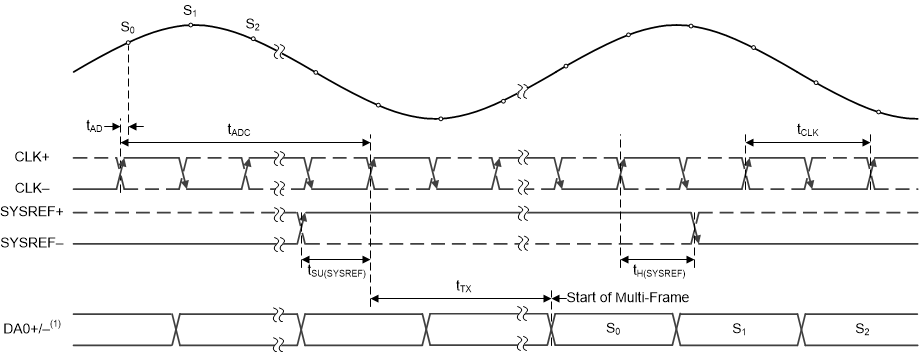
| tAD | Sampling (aperture) delay from CLK+/- rising edge (dual channel mode) or rising and falling edge (single channel mode) to sampling instant | TAD_COARSE = 0x00, TAD_FINE = 0x00 and TAD_INV = 0 | 360 | ps | ||
| tTAD(MAX) | Maximum tAD Adjust programmable delay, not including clock inversion (TAD_INV = 0) | Coarse adjustment (TAD_COARSE = 0xFF) | 289 | ps | ||
| Fine adjustment (TAD_FINE = 0xFF) | 4.9 | ps | ||||
| tTAD(STEP) | tAD Adjust programmable delay step size | Coarse adjustment (TAD_COARSE) | 1.13 | ps | ||
| Fine adjustment (TAD_FINE) | 19 | fs | ||||
| tAJ | Aperture jitter, rms | Minimum tAD Adjust coarse setting (TAD_COARSE = 0x00, TAD_INV = 0) | 50 | fs | ||
| Maximum tAD Adjust coarse setting (TAD_COARSE = 0xFF) excluding TAD_INV (TAD_INV = 0) | 70(3) | fs | ||||
| SERIAL DATA OUTPUTS (DA0+...DA7+, DA0–...DA7–, DB0+...DB7+, DB0–...DB7–) | ||||||
| fSERDES | Serialized output bit rate | 1 | 12.8 | Gbps | ||
| UI | Serialized output unit interval | 78.125 | 1000 | ps | ||
| tTLH | Low-to-high transition time (differential) | 20% to 80%, PRBS-7 test pattern, 12.8 Gbps, SER_PE = 0x04 | 37 | ps | ||
| tTHL | High-to-low transition time (differential) | 20% to 80%, PRBS-7 test pattern, 12.8 Gbps, SER_PE = 0x04 | 37 | ps | ||
| DDJ | Data dependent jitter, peak-to-peak | PRBS-7 test pattern, 12.8 Gbps, SER_PE = 0x04, JMODE = 2 | 7.8 | ps | ||
| RJ | Random jitter, RMS | PRBS-7 test pattern, 12.8 Gbps, SER_PE = 0x04, JMODE = 2 | 1.1 | ps | ||
| TJ | Total jitter, peak-to-peak, with gaussian portion defined with respect to a BER=1e-15 (Q=7.94) | PRBS-7 test pattern, 12.8 Gbps, SER_PE = 0x04, JMODE = 0, 2 | 25 | ps | ||
| PRBS-7 test pattern, 6.4 Gbps, SER_PE = 0x04, JMODE = 1, 3 | 21 | ps | ||||
| PRBS-7 test pattern, 8 Gbps, SER_PE = 0x04, JMODE = 4, 5, 6, 7 | 28 | ps | ||||
| PRBS-7 test pattern, 8 Gbps, SER_PE = 0x04, JMODE = 9 | 35 | ps | ||||
| PRBS-7 test pattern, 8 Gbps, SER_PE = 0x04, JMODE = 10, 11 | 40 | ps | ||||
| PRBS-7 test pattern, 3.2 Gbps, SER_PE = 0x04, JMODE = 12 | 26 | ps | ||||
| PRBS-7 test pattern, 8 Gbps, SER_PE = 0x04, JMODE = 13, 14 | 39 | ps | ||||
| PRBS-7 test pattern, 8 Gbps, SER_PE = 0x04, JMODE = 15, 16 | 34 | ps | ||||
| ADC CORE LATENCY | ||||||
| tADC | Deterministic delay from the CLK+/– edge that samples the reference sample to the CLK+/– edge that samples SYSREF going high(1) | JMODE = 0 | -8.5 | tCLK cycles | ||
| JMODE = 1 | -20.5 | |||||
| JMODE = 2 | -9 | |||||
| JMODE = 3 | -21 | |||||
| JMODE = 4 | -4.5 | |||||
| JMODE = 5 | -24.5 | |||||
| JMODE = 6 | -5 | |||||
| JMODE = 7 | -25 | |||||
| JMODE = 9 | 60 | |||||
| JMODE = 10 | 140 | |||||
| JMODE = 11 | 136 | |||||
| JMODE = 12 | 120 | |||||
| JMODE = 13 | 232 | |||||
| JMODE = 14 | 232 | |||||
| JMODE = 15 | 446 | |||||
| JMODE = 16 | 430 | |||||
| JMODE = 17 | -48.5 | |||||
| JMODE = 18 | -49 | |||||
| JESD204B AND SERIALIZER LATENCY | ||||||
| tTX | Delay from the CLK+/– rising edge that samples SYSREF high to the first bit of the multi-frame on the JESD204B serial output lane corresponding to the reference sample of tADC(2) | JMODE = 0 | 72 | 84 | tCLK cycles | |
| JMODE = 1 | 119 | 132 | ||||
| JMODE = 2 | 72 | 84 | ||||
| JMODE = 3 | 119 | 132 | ||||
| JMODE = 4 | 67 | 80 | ||||
| JMODE = 5 | 106 | 119 | ||||
| JMODE = 6 | 67 | 80 | ||||
| JMODE = 7 | 106 | 119 | ||||
| JMODE = 9 | 106 | 119 | ||||
| JMODE = 10 | 67 | 80 | ||||
| JMODE = 11 | 106 | 119 | ||||
| JMODE = 12 | 213 | 225 | ||||
| JMODE = 13 | 67 | 80 | ||||
| JMODE = 14 | 106 | 119 | ||||
| JMODE = 15 | 67 | 80 | ||||
| JMODE = 16 | 106 | 119 | ||||
| JMODE = 17 | 195 | 208 | ||||
| JMODE = 18 | 195 | 208 | ||||
| SERIAL PROGRAMMING INTERFACE (SDO) | ||||||
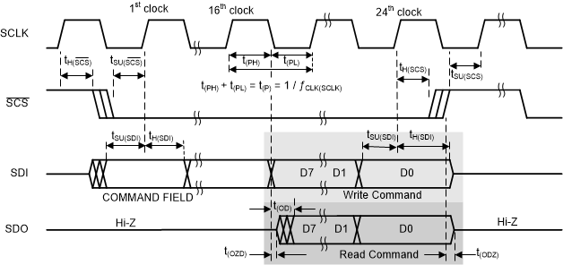
| t(OZD) | Maximum delay from falling edge of 16th SCLK cycle during read operation for SDO transition from tri-state to valid data | 7 | ns | |||
| t(ODZ) | Maximum delay from SCS rising edge for SDO transition from valid data to tri-state | 7 | ns | |||
| t(OD) | Maximum delay from falling edge of 16th SCLK cycle during read operation to SDO valid | 12 | ns | |||
(1) tADC is an exact, unrounded, deterministic delay. The delay can be negative if the reference sample is sampled after the SYSREF high capture point, in which case the total latency is smaller than the delay given by tTX.
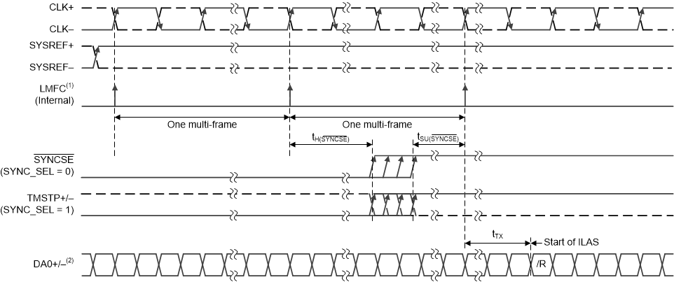
(2) The values given for tTX include deterministic and non-deterministic delays. Over process, temperature, and voltage, the delay will vary. JESD204B accounts for these variations when operating in subclass-1 mode in order to achieve deterministic latency. Proper receiver RBD value must be chosen such that the elastic buffer release point does not occur within the invalid region of the local multi-frame clock (LMFC) cycle.
(3) tAJ increases due to additional attenuation on internal clock path.

1. Only the SerDes lane DA0± is shown, but DA0± is representative of all lanes. The number of output lanes used and bit-packing format is dependent on the programmed JMODE value.
Figure 1. ADC Timing Diagram 
1. The internal LMFC is assumed to be aligned with the CLK± rising edge that captures the SYSREF± high value.
2. Only SerDes lane DA0± is shown, but DA0± is representative of all lanes. All lanes output /R at approximately the same point in time. The number of lanes is dependent on the programmed JMODE value.
Figure 2. SYNCSE and TMSTP± Timing Diagram for NCO Synchronization  Figure 3. Serial Interface Timing