JAJSDX8E June 2017 – August 2018 ISO1211 , ISO1212
PRODUCTION DATA.
- 1 特長
- 2 アプリケーション
- 3 概要
- 4 改訂履歴
- 5 概要(続き)
- 6 Pin Configuration and Functions
-
7 Specifications
- 7.1 Absolute Maximum Ratings
- 7.2 ESD Ratings
- 7.3 Recommended Operating Conditions
- 7.4 Thermal Information
- 7.5 Power Ratings
- 7.6 Insulation Specifications
- 7.7 Safety-Related Certifications
- 7.8 Safety Limiting Values
- 7.9 Electrical Characteristics—DC Specification
- 7.10 Switching Characteristics—AC Specification
- 7.11 Insulation Characteristics Curves
- 7.12 Typical Characteristics
- 8 Parameter Measurement Information
- 9 Detailed Description
-
10Application and Implementation
- 10.1 Application Information
- 10.2
Typical Application
- 10.2.1
Sinking Inputs
- 10.2.1.1 Design Requirements
- 10.2.1.2
Detailed Design Procedure
- 10.2.1.2.1 Setting Current Limit and Voltage Thresholds
- 10.2.1.2.2 Thermal Considerations
- 10.2.1.2.3 Designing for 48-V Systems
- 10.2.1.2.4 Designing for Input Voltages Greater Than 60 V
- 10.2.1.2.5 Surge, ESD, and EFT Tests
- 10.2.1.2.6 Multiplexing the Interface to the Host Controller
- 10.2.1.2.7 Status LEDs
- 10.2.1.3 Application Curve
- 10.2.2 Sourcing Inputs
- 10.2.3 Sourcing and Sinking Inputs (Bidirectional Inputs)
- 10.2.1
Sinking Inputs
- 11Power Supply Recommendations
- 12Layout
- 13デバイスおよびドキュメントのサポート
- 14メカニカル、パッケージ、および注文情報
10.1 Application Information
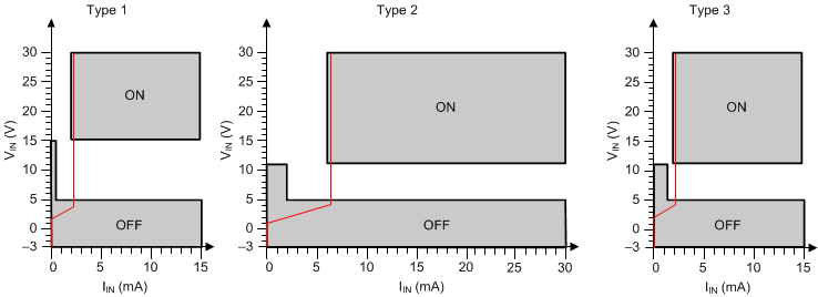
The ISO1211 and ISO1212 devices are fully-integrated, isolated digital-input receivers with IEC 61131-2 Type 1, 2, and 3 characteristics. These devices are suitable for high-channel density, digital-input modules for programmable logic controllers and motor control digital input modules. The devices receive 24-V to 60-V digital-input signals and provide isolated digital outputs. No field side power supply is required. An external resistor, RSENSE, on the input signal path precisely sets the limit for the current drawn from the field input. This current limit helps minimize power dissipated in the system. The current limit can be set for Type 1, 2, or 3 operation. The voltage transition thresholds are compliant with Type 1, 2, and 3 and can be increased further using an external resistor, RTHR. For more information on selecting the RSENSE and RTHR resistor values, see the Detailed Design Procedure section. The ISO1211 and ISO1212 devices are capable of high speed operation and can pass through a minimum pulse width of 150 ns. The ISO1211 device has a single receive channel. The ISO1212 device has two receive channels that are independent on the field side.
 Figure 15. Switching Characteristics for IEC61131-2 Type 1, 2, and 3 Proximity Switches