JAJSE45C February 2016 – December 2021 SN65DP141
PRODUCTION DATA
- 1 特長
- 2 アプリケーション
- 3 概要
- 4 Revision History
- 5 Pin Configuration and Functions
- 6 Specifications
- 7 Parameter Measurement Information
-
8 Detailed Description
- 8.1 Overview
- 8.2 Functional Block Diagram
- 8.3 Feature Description
- 8.4 Device Functional Modes
- 8.5
Register Maps
- 8.5.1 Register 0x00 (General Device Settings) (offset = 00000000) [reset = 00000000]
- 8.5.2 Register 0x01 (Channel Enable) (offset = 00000000) [reset = 00000000]
- 8.5.3 Register 0x02 (Channel 0 Control Settings) (offset = 00000000) [reset = 00000000]
- 8.5.4 Register 0x03 (Channel 0 Enable Settings) (offset = 00000000) [reset = 00000000]
- 8.5.5 Register 0x05 (Channel 1 Control Settings) (offset = 00000000) [reset = 00000000]
- 8.5.6 Register 0x06 (Channel 1 Enable Settings) (offset = 00000000) [reset = 00000000]
- 8.5.7 Register 0x08 (Channel 2 Control Settings) (offset = 00000000) [reset = 00000000]
- 8.5.8 Register 0x09 (Channel 2 Enable Settings) (offset = 00000000) [reset = 00000000]
- 8.5.9 Register 0x0B (Channel 3 Control Settings) (offset = 00000000) [reset = 00000000]
- 8.5.10 Register 0x0C (Channel 3 Control Settings) (offset = 00000000) [reset = 00000000]
- 9 Application and Implementation
- 10Power Supply Recommendations
- 11Layout
- 12Device and Documentation Support
- 13Mechanical, Packaging, and Orderable Information
7 Parameter Measurement Information
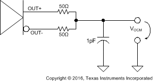 Figure 7-1 Common
Mode Output Voltage Test Circuit
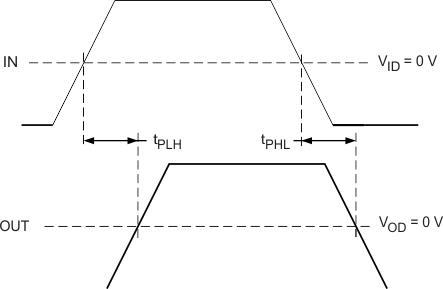 Figure 7-2 Propagation Delay Input to Output
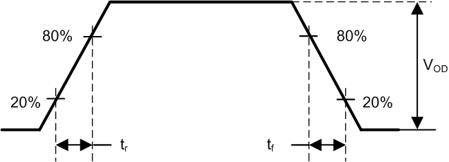 Figure 7-3 Output
Rise and Fall Times
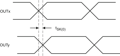 Figure 7-4 Output
Inter-Pair Skew
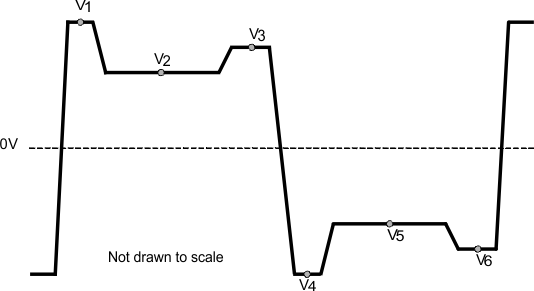 Figure 7-5 V(pre) and V(post) (test pattern is 1111111100000000
(8-1s, 8-0s))
 Figure 7-6 Receive
Side Performance Test Circuit
 Figure 7-7 Transmit
Side Performance Test Circuit
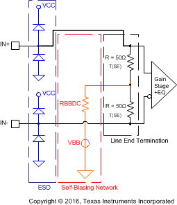 Figure 7-8 Equivalent Input Circuit
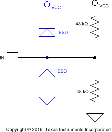 Figure 7-9 3-Level
Input Biasing Network
 Figure 7-10 Two –
Wire Serial Interface Data Transfer
 Figure 7-11 Two –
Wire Serial Interface Timing Diagram