JAJSHF7A May 2019 – November 2019 AMC1035-Q1
PRODUCTION DATA.
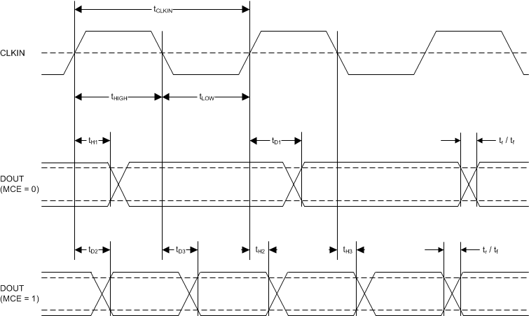
6.5 Switching Characteristics
| PARAMETER | TEST CONDITIONS | MIN | TYP | MAX | UNIT | |
|---|---|---|---|---|---|---|
| fCLK | CLKIN clock frequency | MCE = 0 | 9 | 20 | 21 | MHz |
| MCE = 1 | 9 | 10 | 11 | |||
| DutyCycle | CLKIN duty cycle | 40% | 50% | 60% | ||
| tH1 | DOUT hold time after rising edge of CLKIN | MCE = 0, CLOAD = 15 pF | 6 | ns | ||
| tH2 | DOUT hold time after rising edge of CLKIN | MCE = 1, CLOAD = 15 pF | 6 | 23 | ns | |
| tH3 | DOUT hold time after falling edge of CLKIN | MCE = 1, CLOAD = 15 pF | 10 | 26 | ns | |
| tD1 | Rising edge of CLKIN to DOUT valid delay | MCE = 0, CLOAD = 15 pF | 25 | ns | ||
| tD2 | Rising edge of CLKIN to DOUT valid delay | MCE = 1, CLOAD = 15 pF | 11 | 27 | ns | |
| tD3 | Falling edge of CLKIN to DOUT valid delay | MCE = 1, CLOAD = 15 pF | 15 | 30 | ns | |
| tr | DOUT rise time | 10% to 90%, 3.0 V ≼ VDD ≼ 3.6 V, CLOAD = 15 pF | 2.5 | 5 | ns | |
| 10% to 90%, 4.5 V ≼ VDD ≼ 5.5 V, CLOAD = 15 pF | 1.5 | 3.5 | ||||
| tf | DOUT fall time | 10% to 90%, 3.0 V ≼ VDD ≼ 3.6 V, CLOAD = 15 pF | 2.5 | 5.8 | ns | |
| 10% to 90%, 4.5 V ≼ VDD ≼ 5.5 V,CLOAD = 15 pF | 1.8 | 4.4 | ||||
| tASTART | Analog startup time | VDD step to 3.0 V; 0.1%-settling, clock applied | 0.25 | ms | ||
 Figure 1. Digital Interface Timing
  Figure 2. Device Startup Timing