JAJSIJ6F April 2011 – February 2020 AMC1204
PRODUCTION DATA.
- 1 特長
- 2 アプリケーション
- 3 概要
- 4 改訂履歴
- 5 概要(続き)
- 6 Pin Configuration and Functions
-
7 Specifications
- 7.1 Absolute Maximum Ratings
- 7.2 ESD Ratings
- 7.3 Recommended Operating Conditions
- 7.4 Thermal Information
- 7.5 Power Ratings
- 7.6 Insulation Specifications
- 7.7 Safety-Related Certifications
- 7.8 Safety Limiting Values
- 7.9 Electrical Characteristics
- 7.10 Timing Requirements
- 7.11 Insulation Characteristics Curves
- 7.12 Typical Characteristics
- 8 Detailed Description
- 9 Application and Implementation
- 10Power Supply Recommendations
- 11Layout
- 12デバイスおよびドキュメントのサポート
- 13メカニカル、パッケージ、および注文情報
6 Pin Configuration and Functions
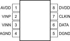
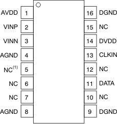
Pin Functions
| PIN | I/O | DESCRIPTION | ||
|---|---|---|---|---|
| NAME | NO. | |||
| 8 PINS | 16 PINS | |||
| AVDD | 1 | 1 | Power | High-side power supply |
| VINP | 2 | 2 | Analog input | Noninverting analog input |
| VINN | 3 | 3 | Analog input | Inverting analog input |
| AGND | 4 | 4, 8(1) | Power | High-side ground |
| DGND | 5 | 9, 16 | Power | Controller-side ground |
| DATA | 6 | 11 | Digital output | Modulator data output |
| CLKIN | 7 | 13 | Digital input | Modulator clock input |
| DVDD | 8 | 14 | Power | Controller-side power supply |
| NC | — | 5-7, 10, 12, 15 | — | No internal connection; can be tied to any potential or left unconnected |
(1) Both pins are connected internally via a low-impedance path; thus, only one of the pins must be tied to the ground plane.

