JAJSJ98B June   2020  – April 2022 UCC27288

PRODUCTION DATA  

  1. 特長
  2. アプリケーション
  3. 説明
  4. Revision History
  5. Pin Configuration and Functions
  6. Specifications
    1. 6.1 Absolute Maximum Ratings
    2. 6.2 ESD Ratings
    3. 6.3 Recommended Operating Conditions
    4. 6.4 Thermal Information
    5. 6.5 Electrical Characteristics
    6. 6.6 Switching Characteristics
    7. 6.7 Typical Characteristics
  7. Detailed Description
    1. 7.1 Overview
    2. 7.2 Functional Block Diagram
    3. 7.3 Feature Description
      1. 7.3.1 Start-up and UVLO
      2. 7.3.2 Input Stages
      3. 7.3.3 Level Shifter
      4. 7.3.4 Output Stage
      5. 7.3.5 Negative Voltage Transients
    4. 7.4 Device Functional Modes
  8. Application and Implementation
    1. 8.1 Application Information
    2. 8.2 Typical Application
      1. 8.2.1 Design Requirements
      2. 8.2.2 Detailed Design Procedure
        1. 8.2.2.1 Select Bootstrap and VDD Capacitor
        2. 8.2.2.2 External Bootstrap Diode and Series Resistor
        3. 8.2.2.3 Estimate Driver Power Losses
        4. 8.2.2.4 Selecting External Gate Resistor
        5. 8.2.2.5 Delays and Pulse Width
        6. 8.2.2.6 VDD and Input Filter
        7. 8.2.2.7 Transient Protection
      3. 8.2.3 Application Curves
  9. Power Supply Recommendations
  10. 10Layout
    1. 10.1 Layout Guidelines
    2. 10.2 Layout Example
  11. 11Device and Documentation Support
    1. 11.1 ドキュメントの更新通知を受け取る方法
    2. 11.2 サポート・リソース
    3. 11.3 Trademarks
    4. 11.4 静電気放電に関する注意事項
    5. 11.5 用語集
  12. 12Mechanical, Packaging, and Orderable Information

Typical Characteristics

Unless otherwise specified VVDD=VHB = 12 V, VHS=VVSS = 0 V, No load on outputs
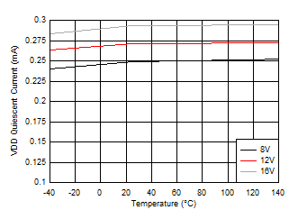
GUID-9036C1B4-4ED0-42D5-AFAF-09889A043280-low.gif
VHI = VLI = 0 V
Figure 6-2 VDD Quiescent Current
GUID-E5AF7BAE-0285-462D-A2A1-77DBE4F11575-low.gif
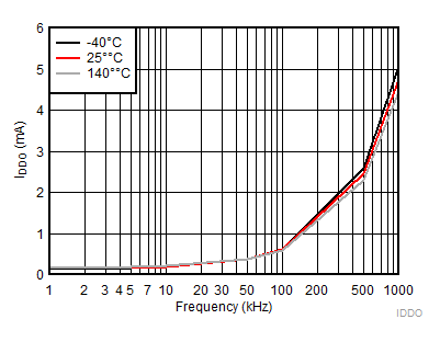
CL = 0 F VDD =VHB= 12V
Figure 6-4 VDD Operating Current
GUID-9227104E-7872-4F67-9C73-CFD5C29E1453-low.gif
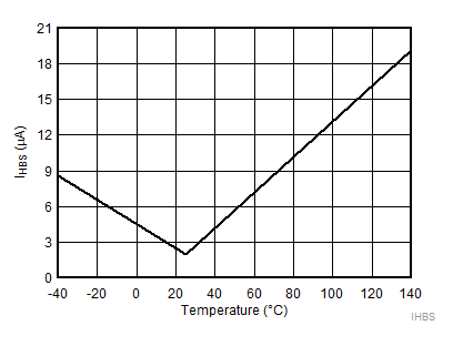
VHB=VHS=100V
Figure 6-6 HB to VSS Quiescent Current
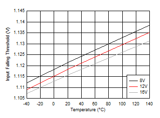
GUID-A37960F0-749D-4163-8F04-44BDB903742A-low.gifFigure 6-8 Input Falling Threshold
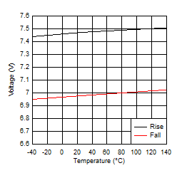
GUID-9865D931-080E-4FDE-8219-44E018FA3016-low.gifFigure 6-10 VDD UVLO Threshold
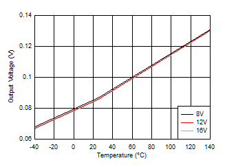
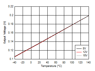
GUID-764AFB16-51D8-4D11-9C46-E2C464081017-low.gif
IO=100mA
Figure 6-12 LO Low Output Voltage (VLOL)
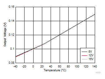
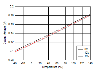
GUID-4BFCDA2C-CDEA-4E1C-9E58-17B496F8608E-low.gif
IO=100mA
Figure 6-14 HO Low Output Voltage (VHOL)
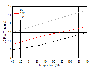
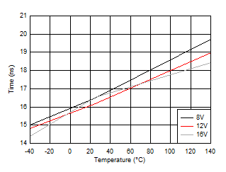
GUID-EA981292-32C0-4974-A8A0-1168DC1FE080-low.gif
CL=1800pF
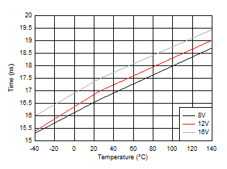
Figure 6-16 LO Rise Time
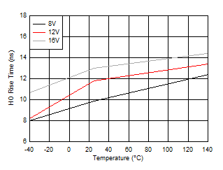
GUID-4FAE75A7-EDF1-4E00-A2DC-D8FC28E03240-low.gif
CL=1800pF
Figure 6-18 HO Rise Time
GUID-4F7D87F5-FDEF-47D9-A6F7-67F061A37418-low.gif
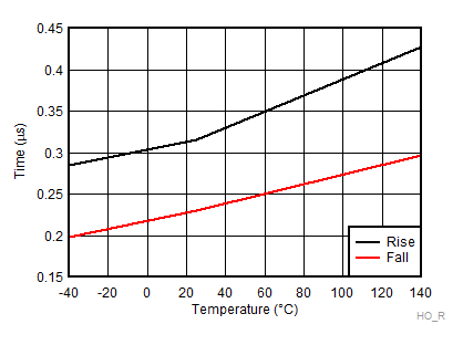
CL=100nF VDD = 12 V
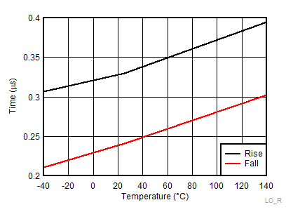
Figure 6-20 LO Rise & Fall Time
GUID-33A01B0A-97FD-4F3A-AF9E-C14375EFC98C-low.gif
CL=No Load
Figure 6-22 HO Rising Propagation Delay (TDHRR)
GUID-513811CA-9551-4E35-A2C7-672C308CD0DF-low.gif
CL= No Load
Figure 6-24 LO Rising Propagation Delay (TDLRR)
GUID-1A5CA6C6-0A11-4880-9759-F11AE1D146EE-low.gif
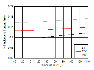
VHI = VLI = 0 V
Figure 6-3 HB Quiescent Current
GUID-E2197D18-6F87-42CC-A9BD-2D81FA592C2D-low.gif
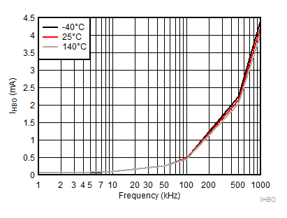
CL = 0 F VDD =VHB= 12V
Figure 6-5 HB Operating Current
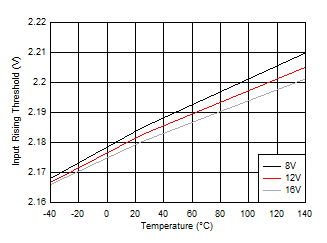
GUID-505E33E6-C88D-4B5A-9090-B9F49DA16339-low.gifFigure 6-7 Input Rising Threshold
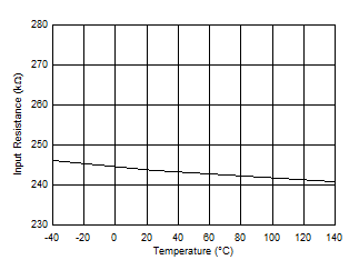
GUID-6082C9A7-CCA7-4E91-BF96-0F196207BDEB-low.gifFigure 6-9 Input Pull-down Resistor
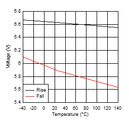
GUID-92FAA77A-B866-4412-B636-9D73177B4017-low.gifFigure 6-11 HB UVLO Threshold
GUID-37285CD9-798E-4689-965C-34C3AA7E189A-low.gif
IO=-100mA
Figure 6-13 LO High Output Voltage (VLOH)
GUID-E0AFE00C-E3E8-48B5-B5F3-189BDE306BB2-low.gif
IO=-100mA
Figure 6-15 HO High Output Voltage (VHOH)
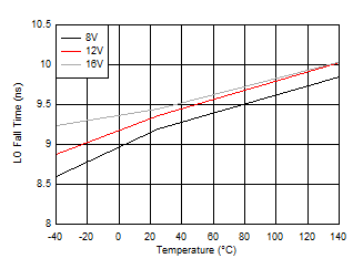
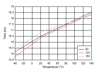
GUID-16F6673E-49D2-4811-B39B-493E5A607992-low.gif
CL=1800pF
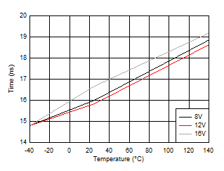
Figure 6-17 LO Fall Time
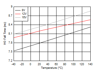
GUID-58334D73-4442-44D4-AF81-69EFA7F50DA9-low.gif
CL=1800pF
Figure 6-19 HO Fall Time
GUID-72D40EBF-3F88-49E4-89B8-5C44CB242036-low.gif
CL=100nF VDD = 12 V
Figure 6-21 HO Rise & Fall Time
GUID-BB67FACD-1050-4BCA-886A-009CFF03A89C-low.gif
CL= No Load
Figure 6-23 HO Falling Propagation Delay (TDHFF)
GUID-ECAC3118-3332-441B-B7D4-BD214F98FBB3-low.gif
CL= No Load
Figure 6-25 LO Falling Propagation Delay (TDLFF)