JAJSJV7C december   2020  – may 2023 TPS272C45

PRODUCTION DATA  

  1.   1
  2. 特長
  3. アプリケーション
  4. 概要
  5. Revision History
  6. Device Comparison Table
  7. Pin Configuration and Functions
    1. 6.1 Recommended Connections for Unused Pins
  8. Specifications
    1. 7.1 Absolute Maximum Ratings
    2. 7.2 ESD Ratings
    3. 7.3 Recommended Operating Conditions
    4. 7.4 Thermal Information
    5. 7.5 Electrical Characteristics
    6. 7.6 SNS Timing Characteristics
    7. 7.7 Switching Characteristics
    8. 7.8 Typical Characteristics
  9. Parameter Measurement Information
  10. Detailed Description
    1. 9.1 Overview
    2. 9.2 Functional Block Diagram
    3. 9.3 Feature Description
      1. 9.3.1 Programmable Current Limit
        1. 9.3.1.1 Inrush Current Handling
        2. 9.3.1.2 Calculating RILIMx
        3. 9.3.1.3 Configuring ILIMx From an MCU
      2. 9.3.2 Low Power Dissipation
      3. 9.3.3 Protection Mechanisms
        1. 9.3.3.1 Short-Circuit Protection
          1. 9.3.3.1.1 VS During Short-to-Ground
        2. 9.3.3.2 Inductive Load Demagnetization
        3. 9.3.3.3 Thermal Shutdown
        4. 9.3.3.4 Undervoltage Lockout on VS (UVLO)
        5. 9.3.3.5 Undervoltage Lockout on Low Voltage Supply (VDD_UVLO)
        6. 9.3.3.6 Power-Up and Power-Down Behavior
        7. 9.3.3.7 Overvoltage Protection (OVPR)
      4. 9.3.4 Diagnostic Mechanisms
        1. 9.3.4.1 Current Sense
          1. 9.3.4.1.1 RSNS Value
            1. 9.3.4.1.1.1 Current Sense Output Filter
        2. 9.3.4.2 Fault Indication
          1. 9.3.4.2.1 Fault Event Diagrams
        3. 9.3.4.3 Short-to-Supply or Open-Load Detection
          1. 9.3.4.3.1 Detection With Switch Enabled
          2. 9.3.4.3.2 Detection With Switch Disabled
        4. 9.3.4.4 Current Sense Resistor Sharing
    4. 9.4 Device Functional Modes
      1. 9.4.1 Off
      2. 9.4.2 Diagnostic
      3. 9.4.3 Active
      4. 9.4.4 Fault
  11. 10Application and Implementation
    1. 10.1 Application Information
      1. 10.1.1 IEC 61000-4-5 Surge
      2. 10.1.2 Inverse Current
      3. 10.1.3 Loss of GND
      4. 10.1.4 Paralleling Channels
      5. 10.1.5 Thermal Information
    2. 10.2 Typical Application
      1. 10.2.1 Design Requirements
      2. 10.2.2 Detailed Design Procedure
        1. 10.2.2.1 RILIM Calculation
        2. 10.2.2.2 Diagnostics
          1. 10.2.2.2.1 Selecting the RISNS Value
      3. 10.2.3 Application Curves
    3. 10.3 Power Supply Recommendations
    4. 10.4 Layout
      1. 10.4.1 Layout Guidelines
      2. 10.4.2 Layout Example
  12. 11Device and Documentation Support
    1. 11.1 Documentation Support
      1. 11.1.1 Related Documentation
    2. 11.2 ドキュメントの更新通知を受け取る方法
    3. 11.3 サポート・リソース
    4. 11.4 Trademarks
    5. 11.5 静電気放電に関する注意事項
    6. 11.6 用語集
  13. 12Mechanical, Packaging, and Orderable Information

Typical Characteristics

GUID-20211118-SS0I-XN2H-6DTW-Q4WXCGWHJRSM-low.svg
VDD = 3.3 VVEN = 3.3 VVDIA_EN = 0 V
ROUT = open
Figure 7-1 Quiescent Current (IQ_VS_DS) From VS Input Supply vs Temperature
GUID-20211118-SS0I-9GSR-2PR5-3WS8RLW3QRKR-low.svg

VDD = 0 V

VEN = 5 VVDIA_EN = 0 V
ROUT = open
Figure 7-3 Quiescent Current (IQ_VS_SS) From VS Input Supply vs Temperature
GUID-20211118-SS0I-QGB5-BXNM-Z9SCL8SH7KB7-low.svg
VS = 24 VVEN = 0 V to 5 VVDIA_EN = 0 V
ROUT = 48 Ω
Figure 7-5 Turn-on Time (tON) vs Temperature
GUID-20211118-SS0I-RHJG-Q5N2-ZZ5W2ZGW3SWR-low.svg

VS = 24 V, 30 V

VEN = 5 VVDIA_EN = 5 V
RSNS = 1 kΩ
Figure 7-7 Current Sense Output Current (ISNSI) vs Load Current (IOUT) Across Temperature
GUID-20211118-SS0I-QV5R-3PNQ-FLCH19NPJC7L-low.svg
VS = 24 VVEN = 5 VVDIA_EN = 0 V
ROUT = open
Figure 7-2 Quiescent Current (IQ_VDD_DS) From VDD Input Supply vs Temperature
GUID-20211118-SS0I-NMPV-R0MX-D7Q8Q0WSGFML-low.svg
IOUT = 200 mAVEN = 5 VVDIA_EN = 0 V
Figure 7-4 On Resistance (RON) vs Temperature
GUID-20211118-SS0I-DRGS-KSFP-ZXDZJ5DTBQ4M-low.svg
VS = 24 VVEN = 0 V to 5 VVDIA_EN = 0 V
ROUT = 48 Ω
Figure 7-6 Turn-off Time (tOFF) vs Temperature
GUID-20211119-SS0I-S5BB-6ZLZ-KCNKG5TG3CXR-low.svg

VS = 24 V

VDIA_EN = 0 VROUT = 1 kΩ
Figure 7-8 VIH, VIL vs Temperature
GUID-20211116-SS0I-BP5F-WNX7-PVLRX1D437NL-low.png
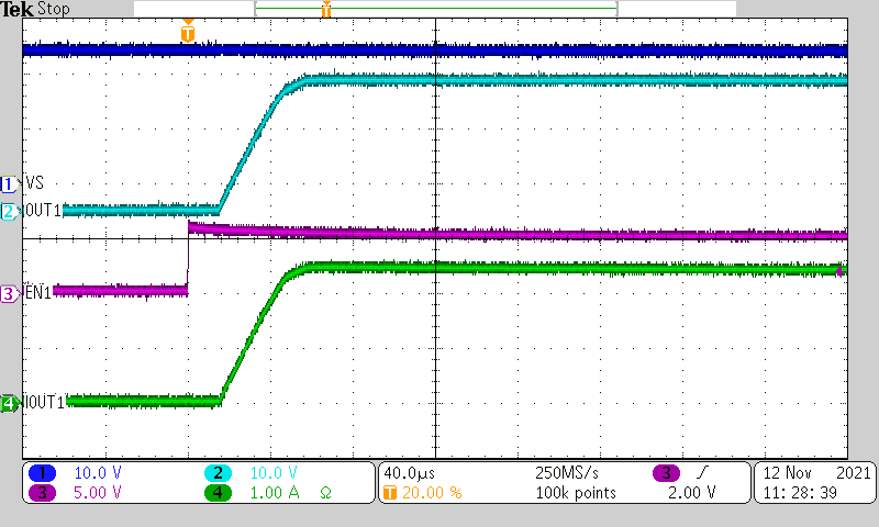
VEN = 0 V to 5 VVS = 24 VROUT = 10 Ω
Figure 7-9 Turn-on Time (TON)
GUID-20211116-SS0I-FKQB-M0J5-M2JMHRFZT1M9-low.png
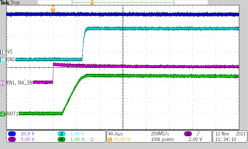
VEN = VDIAG_EN = 0 V to 5 VVS = 24 VROUT = 10 Ω
Figure 7-11 ISNS Settling Time on DIA_EN Transition
GUID-20211116-SS0I-NL3N-07ZZ-C1BKBFBHQKKW-low.png
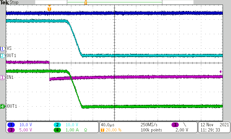
VEN = 5 V to 0 VVS = 24 VROUT = 10 Ω
Figure 7-10 Turn-off Time (TOFF)
GUID-20211116-SS0I-F0Z0-WSRH-MH6PLJLKJFRP-low.png
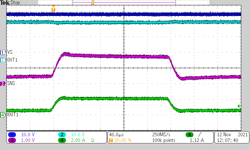
VEN = 5 VVDIAG_EN = 5 VIOUT1 = 0.5 A to 2 A
Figure 7-12 ISNS Settling Time on Rising Load Step