JAJSK72A june 2020 – october 2020 UCC23514
PRODUCTION DATA
- 1
- 1 特長
- 2 アプリケーション
- 3 概要
- 4 Revision History
- 5 Pin Configuration and Function
-
6 Specifications
- 6.1 Absolute Maximum Ratings
- 6.2 ESD Ratings
- 6.3 Recommended Operating Conditions
- 6.4 Thermal Information
- 6.5 Power Ratings
- 6.6 Insulation Specifications
- 6.7 Safety-Related Certifications
- 6.8 Safety Limiting Values
- 6.9 Electrical Characteristics
- 6.10 Switching Characteristics
- 6.11 Insulation Characteristics
- 6.12 Typical Characteristics
- 7 Parameter Measurement Information
- 8 Detailed Description
- 9 Application and Implementation
- 10Power Supply Recommendations
- 11Layout
- 12Mechanical, Packaging, and Orderable Information
8.3.3 Output Stage
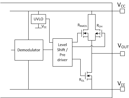
The output stages of the UCC23514 family feature a pullup structure that delivers the highest peak-source current when it is most needed which is during the Miller plateau region of the power-switch turnon transition (when the power-switch drain or collector voltage experiences dV/dt). The output stage pullup structure features a P-channel MOSFET and an additional pull-up N-channel MOSFET in parallel. The function of the N-channel MOSFET is to provide a brief boost in the peak-sourcing current, enabling fast turnon. Fast turnon is accomplished by briefly turning on the N-channel MOSFET during a narrow instant when the output is changing states from low to high. The on-resistance of this N-channel MOSFET (RNMOS) is approximately 5.1 Ω when activated.
| RNMOS | ROH | ROL | UNIT |
|---|---|---|---|
| 5.1 | 9.5 | 0.40 | Ω |
The ROH parameter is a DC measurement and is representative of the on-resistance of the P-channel device only. This parameter is only for the P-channel device because the pullup N-channel device is held in the OFF state in DC condition and is turned on only for a brief instant when the output is changing states from low to high. Therefore, the effective resistance of the UCC23514 pullup stage during this brief turnon phase is much lower than what is represented by the ROH parameter, yielding a faster turn on. The turnon-phase output resistance is the parallel combination ROH || RNMOS.
The pulldown structure in the UCC23514 is simply composed of an N-channel MOSFET. The output voltage swing between VCC and VEE provides rail-to-rail operation because of the MOS-out stage which delivers very low dropout.
 Figure 8-7 Output Stage