JAJSLQ9C February 2016 – August 2021 TPS65981
PRODUCTION DATA
- 1 特長
- 2 アプリケーション
- 3 概要
- 4 Revision History
- 5 概要 (続き)
- 6 Pin Configuration and Functions
-
7 Specifications
- 7.1 Absolute Maximum Ratings
- 7.2 ESD Ratings
- 7.3 Recommended Operating Conditions
- 7.4 Thermal Information
- 7.5 Power Supply Requirements and Characteristics
- 7.6 Power Supervisor Characteristics
- 7.7 Power Consumption Characteristics
- 7.8 Cable Detection Characteristics
- 7.9 USB-PD Baseband Signal Requirements and Characteristics
- 7.10 USB-PD TX Driver Voltage Adjustment Parameter
- 7.11 Port Power Switch Characteristics
- 7.12 Port Data Multiplexer Switching Characteristics
- 7.13 Port Data Multiplexer Clamp Characteristics
- 7.14 Port Data Multiplexer SBU Detection Requirements
- 7.15 Port Data Multiplexer Signal Monitoring Pullup and Pulldown Characteristics
- 7.16 Port Data Multiplexer USB Endpoint Requirements and Characteristics
- 7.17 Port Data Multiplexer BC1.2 Detection Requirements and Characteristics
- 7.18 Analog-to-Digital Converter (ADC) Characteristics
- 7.19 Input-Output (I/O) Requirements and Characteristics
- 7.20 I2C Slave Requirements and Characteristics
- 7.21 SPI Controller Characteristics
- 7.22 BUSPOWERZ Configuration Requirements
- 7.23 Single-Wire Debugger (SWD) Timing Requirements
- 7.24 Thermal Shutdown Characteristics
- 7.25 HPD Timing Requirements and Characteristics
- 7.26 Oscillator Requirements and Characteristics
- 7.27 Typical Characteristics
- 8 Parameter Measurement Information
-
9 Detailed Description
- 9.1 Overview
- 9.2 Functional Block Diagram
- 9.3
Feature Description
- 9.3.1 USB-PD Physical Layer
- 9.3.2 Cable Plug and Orientation Detection
- 9.3.3
Port Power Switches
- 9.3.3.1 5-V Power Delivery
- 9.3.3.2 5V Power Switch as a Source
- 9.3.3.3 PP_5V0 Current Sense
- 9.3.3.4 PP_5V0 Current Limit
- 9.3.3.5 Internal HV Power Delivery
- 9.3.3.6 Internal HV Power Switch as a Source
- 9.3.3.7 Internal HV Power Switch as a Sink
- 9.3.3.8 Internal HV Power Switch Current Sense
- 9.3.3.9 Internal HV Power Switch Current Limit
- 9.3.3.10 External HV Power Delivery
- 9.3.3.11 External HV Power Switch as a Source with RSENSE
- 9.3.3.12 External HV Power Switch as a Sink With RSENSE
- 9.3.3.13 External HV Power Switch as a Sink Without RSENSE
- 9.3.3.14 External Current Sense
- 9.3.3.15 External Current Limit
- 9.3.3.16 Soft Start
- 9.3.3.17 BUSPOWERZ
- 9.3.3.18 Voltage Transitions on VBUS through Port Power Switches
- 9.3.3.19 HV Transition to PP_RV0 Pull-down on VBUS
- 9.3.3.20 VBUS Transition to VSAFE0V
- 9.3.3.21 C_CC1 and C_CC2 Power Configuration and Power Delivery
- 9.3.3.22 PP_CABLE to C_CC1 and C_CC2 Switch Architecture
- 9.3.3.23 PP_CABLE to C_CC1 and C_CC2 Current Limit
- 9.3.4
USB Type-C® Port Data Multiplexer
- 9.3.4.1 USB Top and Bottom Ports
- 9.3.4.2 Multiplexer Connection Orientation
- 9.3.4.3 SBU Crossbar Multiplexer
- 9.3.4.4 Signal Monitoring and Pull-up and Pull-down
- 9.3.4.5 Port Multiplexer Clamp
- 9.3.4.6 USB2.0 Low-Speed Endpoint
- 9.3.4.7 Battery Charger (BC1.2) Detection Block
- 9.3.4.8 BC1.2 Data Contact Detect
- 9.3.4.9 BC1.2 Primary and Secondary Detection
- 9.3.5 Power Management
- 9.3.6 Digital Core
- 9.3.7 USB-PD BMC Modem Interface
- 9.3.8 System Glue Logic
- 9.3.9 Power Reset Congrol Module (PRCM)
- 9.3.10 Interrupt Monitor
- 9.3.11 ADC Sense
- 9.3.12 I2C Slave
- 9.3.13 SPI Controller
- 9.3.14 Single-Wire Debugger Interface
- 9.3.15 DisplayPort HPD Timers
- 9.3.16 ADC
- 9.3.17 I/O Buffers
- 9.3.18 Thermal Shutdown
- 9.3.19 Oscillators
- 9.4 Device Functional Modes
- 9.5 Programming
-
10Application and Implementation
- 10.1 Application Information
- 10.2
Typical Applications
- 10.2.1
Fully-Featured USB Type-C® and PD Charger
Application
- 10.2.1.1 Design Requirements
- 10.2.1.2
Detailed Design Procedure
- 10.2.1.2.1 TPS65981 External Flash
- 10.2.1.2.2 Debug Control (DEBUG_CTL) and I2C (I2C) Resistors
- 10.2.1.2.3 Oscillator (R_OSC) Resistor
- 10.2.1.2.4 VBUS Capacitor and Ferrite Bead
- 10.2.1.2.5 Soft Start (SS) Capacitor
- 10.2.1.2.6 USB Top (C_USB_T), USB Bottom (C_USB_B), and Sideband-Use (SBU) Connections
- 10.2.1.2.7 Port Power Switch (PP_EXT, PP_HV, PP_5V0, and PP_CABLE) Capacitors
- 10.2.1.2.8 Cable Connection (CCn) Capacitors and RPD_Gn Connections
- 10.2.1.2.9 LDO_3V3, LDO_1V8A, LDO_1V8D, LDO_BMC, VIN_3V3, and VDDIO
- 10.2.1.3 Application Curve
- 10.2.2
USB Type-C® and PD Dock or Monitor
Application
- 10.2.2.1 Design Requirements
- 10.2.2.2
Detailed Design Procedure
- 10.2.2.2.1 Port Power Switch (PP_5V0 and PP_CABLE) Capacitors
- 10.2.2.2.2 HD3SS460 Control and DisplayPort Configuration
- 10.2.2.2.3 AC-DC Power Supply (Barrel Jack) Detection Circuitry
- 10.2.2.2.4 TPS65981 Control of Variable Buck Regulator Output Voltage (PP_HV)
- 10.2.2.2.5 TPS65981 and System Controller Interaction
- 10.2.2.3 Application Curves
- 10.2.1
Fully-Featured USB Type-C® and PD Charger
Application
- 11Power Supply Recommendations
-
12Layout
- 12.1
Layout Guidelines
- 12.1.1 TPS65981 Recommended Footprint
- 12.1.2 Top TPS65981 Placement and Bottom Component Placement and Layout
- 12.1.3 Component Placement
- 12.1.4 Designs Rules and Guidance
- 12.1.5 Routing PP_HV, PP_EXT, PP_5V0, and VBUS
- 12.1.6 Routing Top and Bottom Passive Components
- 12.1.7 Thermal Pad Via Placement
- 12.1.8 Top Layer Routing
- 12.1.9 Inner Signal Layer Routing
- 12.1.10 Bottom Layer Routing
- 12.2 Layout Example
- 12.1
Layout Guidelines
- 13Device and Documentation Support
- 14Mechanical, Packaging, and Orderable Information
9.3.4.4 Signal Monitoring and Pull-up and Pull-down
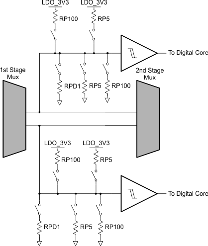
The TPS65981 has comparators that may be enabled to interrupt the core when a switching event occurs on any of the port inputs. The input parameters for the detection are shown in Port Data Multiplexer Signal Monitoring Pullup and Pulldown Characteristics. These comparators are disconnected by application code when these pins are not digital signals but an analog voltage.
The TPS65981 has pull-ups and pull-downs between the first and second stage multiplexers of the port switch for each port output: C_SBU1/2, C_USB_TP/N, C_USB_BP/N. The configurable pull-up and pull-down resistances between each multiplexer are shown in Figure 9-36.
 Figure 9-36 Port Detect and Pull-up and Pull-down