JAJSUC2B December   2015  – April 2024 LDC0851

PRODUCTION DATA  

  1.   1
  2. 特長
  3. アプリケーション
  4. 概要
  5. Pin Configuration and Functions
  6. Specifications
    1. 5.1 Absolute Maximum Ratings
    2. 5.2 ESD Ratings
    3. 5.3 Recommended Operating Conditions
    4. 5.4 Thermal Information
    5. 5.5 Electrical Characteristics
    6. 5.6 Interface Voltage Levels
    7. 5.7 Timing Requirements
    8. 5.8 Typical Characteristics
  7. Detailed Description
    1. 6.1 Overview
    2. 6.2 Functional Block Diagram
    3. 6.3 Feature Description
      1. 6.3.1 Basic Operation Mode
      2. 6.3.2 Threshold Adjust Mode
      3. 6.3.3 Setting the Threshold Adjust Values
      4. 6.3.4 Hysteresis
      5. 6.3.5 Conversion Time
      6. 6.3.6 Power-Up Conditions
    4. 6.4 Device Functional Modes
      1. 6.4.1 Shutdown Mode
      2. 6.4.2 Active Mode
  8. Application and Implementation
    1. 7.1 Application Information
      1. 7.1.1 Sensor Design
        1. 7.1.1.1 Sensor Frequency
        2. 7.1.1.2 Sensor Design Procedure
    2. 7.2 Typical Application
      1. 7.2.1 Event Counting
        1. 7.2.1.1 Design Requirements
        2. 7.2.1.2 Detailed Design Procedure
        3. 7.2.1.3 Application Curves
      2. 7.2.2 Coarse Position Sensing
        1. 7.2.2.1 Design Requirements
        2. 7.2.2.2 Detailed Design Procedure
        3. 7.2.2.3 Application Curves
      3. 7.2.3 Low Power Operation
        1. 7.2.3.1 Design Requirements
        2. 7.2.3.2 Detailed Design Procedure
        3. 7.2.3.3 Application Curves
    3. 7.3 Power Supply Recommendations
    4. 7.4 Layout
      1. 7.4.1 Layout Guidelines
      2. 7.4.2 Layout Example
        1. 7.4.2.1 Side by Side Coils
        2. 7.4.2.2 Stacked Coils
  9. Device and Documentation Support
    1. 8.1 Device Support
      1. 8.1.1 Development Support
    2. 8.2 Documentation Support
      1. 8.2.1 Related Documentation
    3. 8.3 サポート・リソース
    4. 8.4 Trademarks
    5. 8.5 静電気放電に関する注意事項
    6. 8.6 用語集
  10. Revision History
  11. 10Mechanical, Packaging, and Orderable Information

Typical Characteristics

Common test conditions (unless specified otherwise): VDD = 3.3 V, Sense coil diameter = reference coil diameter, Target: Aluminum, 1.5 mm thickness, Target area / Coil area > 100%
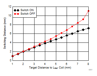
LDC0851 Switching Distance vs. LREF Target Distance
See Basic Operation ModeADJ Code = 0
Coil diameter = 10 mm
Figure 5-1 Switching Distance vs. LREF Target Distance
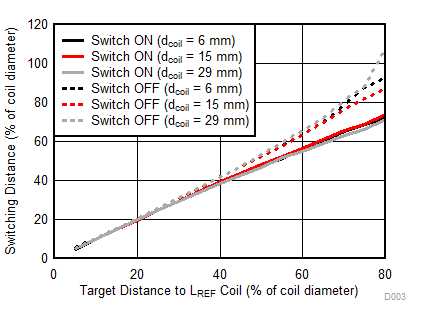
LDC0851 Normalized Switching Distance vs. LREF Target Distance
See Basic Operation ModeADJ Code = 0
Coil diameter = 6 mm, 15 mm, 29 mm
Figure 5-3 Normalized Switching Distance vs. LREF Target Distance
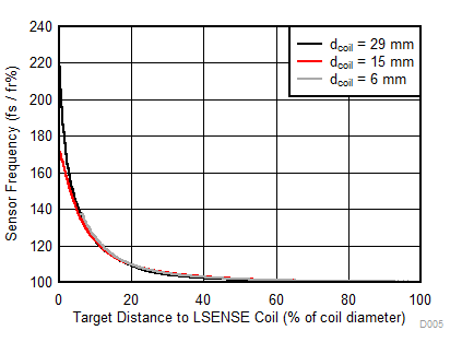
LDC0851 Frequency vs. Distance
LSENSE frequency (fs) variedLREF frequency (fr) fixed
Figure 5-5 Frequency vs. Distance
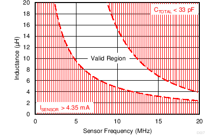
LDC0851 Sensor Design Space for VDD = 1.8 V
ISENSOR_MAX = 4.35 mA
Specified for closest target proximity or minimum inductance in the application.
Figure 5-7 Sensor Design Space for VDD = 1.8 V
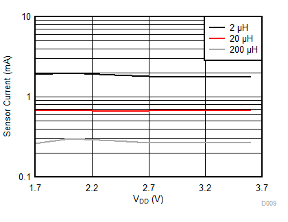
LDC0851 ISENSOR vs. VDD
CTOTAL = 100 pF
Figure 5-9 ISENSOR vs. VDD
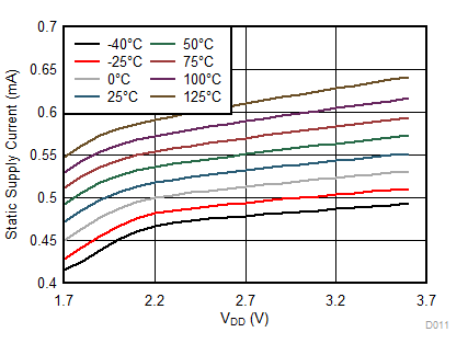
LDC0851 ISTATIC vs. VDDFigure 5-11 ISTATIC vs. VDD
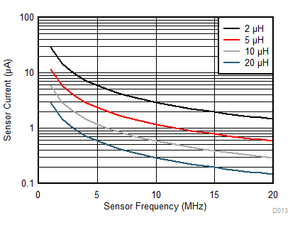
LDC0851 ISENSOR vs. ƒSENSORFigure 5-13 ISENSOR vs. ƒSENSOR
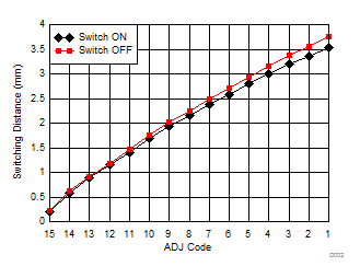
LDC0851 Switching Distance vs. ADJ code
See Threshold Adjust ModeNo reference target
Coil diameter = 10 mm
Figure 5-2 Switching Distance vs. ADJ code
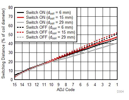
LDC0851 Normalized Switching Distance vs. ADJ Code
See Threshold Adjust ModeNo reference target
Coil diameter = 6 mm, 15 mm, 29 mm
Figure 5-4 Normalized Switching Distance vs. ADJ Code
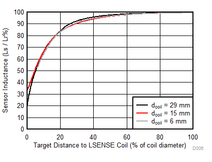
LDC0851 Inductance vs. Distance
LSENSE inductance (Ls) variedLREF inductance (Lr) fixed
Figure 5-6 Inductance vs. Distance
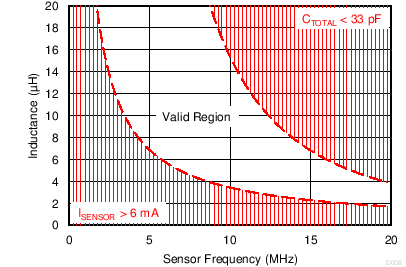
LDC0851 Sensor Design Space for VDD = 3.3 V
ISENSOR_MAX = 6 mA
Specified for closest target proximity or minimum inductance in the application.
Figure 5-8 Sensor Design Space for VDD = 3.3 V
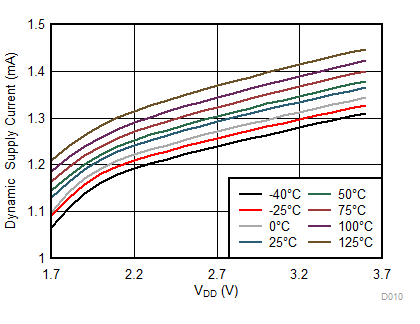
LDC0851 IDYN vs. VDD
CBOARD = 12 pF
ƒSENSOR = 30 MHz
Figure 5-10 IDYN vs. VDD
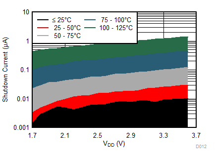
LDC0851 ISD vs. VDDFigure 5-12 ISD vs. VDD
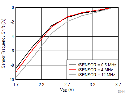
LDC0851 ƒSENSOR Shift vs. VDD
Normalized to frequency at VDD = 3.6 V
Figure 5-14 ƒSENSOR Shift vs. VDD