JAJU459B December 2017 – November 2022
- 概要
- リソース
- 特長
- アプリケーション
- 5
- 1System Description
-
2System Overview
- 2.1 Block Diagram
- 2.2
Design Considerations
- 2.2.1 Conditions of Use: Assumption
- 2.2.2
Diagnostics Coverage
- 2.2.2.1 Dual-Channel Monitoring
- 2.2.2.2 Checking ISO1211 Functionality With MCU (SIL1)
- 2.2.2.3 Checking TPS22919 Functionality With MCU (SIL1)
- 2.2.2.4 Checking TPS27S100 Functionality With MCU (SIL1)
- 2.2.2.5 Optional Monitoring Using RDY Pin of ISO5452, ISO5852S or UCC21750 Integrated Analog-to-PWM Isolated Sensor
- 2.2.3 Drive State
- 2.3 Highlighted Products
- 2.4 System Design Theory
-
3Hardware, Software, Testing Requirements, and Test Results
- 3.1 Getting Started Hardware
- 3.2 Testing and Results
- 4Design Files
- 5Related Documentation
- 6About the Author
- 7Recognition
- 8Revision History
2.4.4 Gate Driver Design
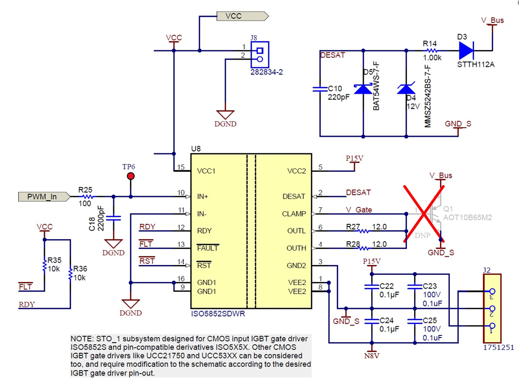
Figure 2-13 shows the schematic design of the isolated gate driver. VCC1 and GND1 are the supply pins for the input side of the ISO5452 or ISO5852S device. The supply voltage at VCC1 can range from 3.0 V to 5.5 V with respect to GND1. VCC2 and GND2 are the supply pins for the output side of the ISO5452 or ISO5852S device. VEE2 is the supply return for the output driver and GND2 is the reference for the logic circuitry. The supply voltage at VCC2 can range from 15 V up to 30 V with respect to VEE2. The PWM is applied across the IN+ and IN– pins of the gate driver.
 Figure 2-13 ISO5852S Schematic
On the secondary-side of the gate driver, gate resistors R27 and R28 control the gate current of the switching device. The DESAT fault detection prevents any destruction resulting from excessive collector currents during a short-circuit fault. To prevent damage to the switching device, the ISO5452, ISO5852S slowly turns off the IGBT in the event of a fault detection. A slow turnoff ensures the overcurrent is reduced in a controlled manner during the fault condition. The DESAT diode D3 conducts the bias current from the gate driver, which allows sensing of the IGBT-saturated collector-to-emitter voltage when the IGBT is in the ON condition. D1 blocks high voltage when the IGBT is in the OFF Condition. In this reference design, D1 blocks a maximum of 1200 V during the IGBT OFF condition. Switching inductive loads causes large, instantaneous forward-voltage transients across the freewheeling diodes of IGBTs. These transients result in a large negative spike in the DESAT pin, which draws substantial current out of the device. To Limit this current below damaging levels, a 1-kΩ resistor is connected in series with the DESAT diode. A 220-pF blanking capacitor C10 is required, which disables the DESAT detection during the OFF-to-ON transition of the power device. For a detailed design procedure, see the Wide-Input Isolated IGBT Gate-Drive Fly-Buck™ Power Supply for Three-Phase Inverters design guide.