JAJU459B December 2017 – November 2022
- 概要
- リソース
- 特長
- アプリケーション
- 5
- 1System Description
-
2System Overview
- 2.1 Block Diagram
- 2.2
Design Considerations
- 2.2.1 Conditions of Use: Assumption
- 2.2.2
Diagnostics Coverage
- 2.2.2.1 Dual-Channel Monitoring
- 2.2.2.2 Checking ISO1211 Functionality With MCU (SIL1)
- 2.2.2.3 Checking TPS22919 Functionality With MCU (SIL1)
- 2.2.2.4 Checking TPS27S100 Functionality With MCU (SIL1)
- 2.2.2.5 Optional Monitoring Using RDY Pin of ISO5452, ISO5852S or UCC21750 Integrated Analog-to-PWM Isolated Sensor
- 2.2.3 Drive State
- 2.3 Highlighted Products
- 2.4 System Design Theory
-
3Hardware, Software, Testing Requirements, and Test Results
- 3.1 Getting Started Hardware
- 3.2 Testing and Results
- 4Design Files
- 5Related Documentation
- 6About the Author
- 7Recognition
- 8Revision History
2.4.5 STO_FB Signal Flow Path
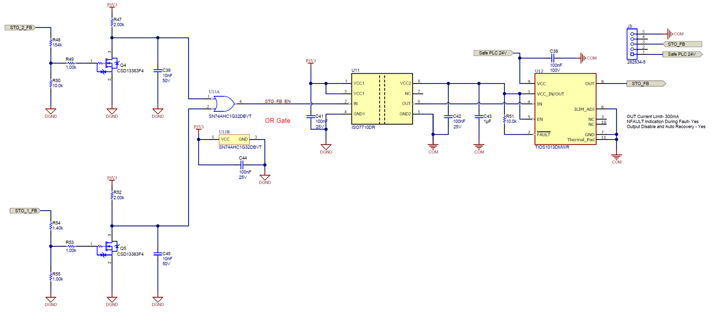
The ISO7710 is a reinforced digital isolator which receives the input signal STO_FB_EN and operates with TIOS1013 (a push-pull driver) to provide feedback signal STO_FB (Logic high = 24 V) to safe PLC. STO_FB_EN is the output signal of the OR gate SN74AHC1G32 which receives the dual-channel feedback signal STO_1_FB and STO_2_FB. Figure 2-14 shows the schematic.
 Figure 2-14 STO_FB Feedback Monitor Schematic
The STO_1_FB is the output of the load switch TPS22919 (controls the primary side VCC1 of the gate driver) and the STO_1_FB connects to the gate of Q5 with the resistors divided network (R54|R55 – 1.4 kΩ|1 kΩ) to synchronize the switching threshold of STO_1_FB with maximum UVLO1 threshold-voltage of gate driver ISO5852S (or ISO5452). According the data sheet of FET Q5 CSD13383F4 and gate driver ISO5852S (or ISO5452), the VGS (th) min = 0.7 V, VIT+(UVLO1) = 2.25 V, then to simulate the switching threshold. The logic 0 (OFF) for STO_1_FB is from 0-V to 2-V and Logic 1 (ON) is from 2 V to 3.9 V (3.9 V is maximum voltage of P3V3). The V GS = 1.37 V during ON state with 1.6-mA IDS current thanks to the limit resistor R52 (2 kΩ).
The STO_2_FB is the output of the load switch TPS27S100 (controls the secondary side VCC2 of gate driver via TIDA-00199 safe power supply) and the STO_2_FB connects to the gate of Q4 with the resistors divided network (R48|R50 – 154 kΩ|10 kΩ) to synchronized the switching threshold of STO_2_FB with maximum UVLO threshold-voltage of the TIDA-00199 design. According the data sheet of FET Q4 CSD13383F4 and TIDA-00199 design guide, the VGS (th) min = 0.7 V, VOFF(UVLO) = 14 V, then to simulate the switching threshold. The logic 0 (OFF) for STO_2_FB is from 0 V to 14 V and Logic 1 (ON) is from 14 V to 28.8 V (28.8 V is maximum voltage of P24-V). The VGS = 1.46 V during ON state with 1.65 mA IDS current due to the limit resistor R47 (2 kΩ).