JAJU510H March   2018  – December 2022


  1.   概要
  2.   リソース
  3.   特長
  4.   アプリケーション
  5.   5
  6. 1System Description
    1. 1.1 Key System Specifications
  7. 2System Overview
    1. 2.1 Block Diagram
    2. 2.2 Highlighted Products
      1. 2.2.1  UCC21710
      2. 2.2.2  UCC5320
      3. 2.2.3  TMS320F28379D
      4. 2.2.4  AMC1305M05
      5. 2.2.5  OPA4340
      6. 2.2.6  LM76003
      7. 2.2.7  PTH08080W
      8. 2.2.8  TLV1117
      9. 2.2.9  OPA350
      10. 2.2.10 UCC14240
    3. 2.3 System Design Theory
      1. 2.3.1 Three-Phase T-Type Inverter
        1. 2.3.1.1 Architecture Overview
        2. 2.3.1.2 LCL Filter Design
        3. 2.3.1.3 Inductor Design
        4. 2.3.1.4 SiC MOSFETs Selection
        5. 2.3.1.5 Loss Estimations
        6. 2.3.1.6 Thermal Considerations
      2. 2.3.2 Voltage Sensing
      3. 2.3.3 Current Sensing
      4. 2.3.4 System Power Supplies
        1. 2.3.4.1 Main Input Power Conditioning
        2. 2.3.4.2 Isolated Bias Supplies
      5. 2.3.5 Gate Drivers
        1. 2.3.5.1 1200-V SiC MOSFETs
        2. 2.3.5.2 650-V SiC MOSFETs
        3. 2.3.5.3 Gate Driver Bias Supply
      6. 2.3.6 Control Design
        1. 2.3.6.1 Current Loop Design
        2. 2.3.6.2 PFC DC Bus Voltage Regulation Loop Design
  8. 3Hardware, Software, Testing Requirements, and Test Results
    1. 3.1 Required Hardware and Software
      1. 3.1.1 Hardware
        1. 3.1.1.1 Test Hardware Required
        2. 3.1.1.2 Microcontroller Resources Used on the Design
        3. 3.1.1.3 F28377D, F28379D Control-Card Settings
      2. 3.1.2 Software
        1. 3.1.2.1 Getting Started With Firmware
          1. 3.1.2.1.1 Opening the CCS project
          2. 3.1.2.1.2 Digital Power SDK Software Architecture
          3. 3.1.2.1.3 Interrupts and Lab Structure
          4. 3.1.2.1.4 Building, Loading and Debugging the Firmware
        2. 3.1.2.2 Protection Scheme
        3. 3.1.2.3 PWM Switching Scheme
        4. 3.1.2.4 ADC Loading
    2. 3.2 Testing and Results
      1. 3.2.1 Lab 1
      2. 3.2.2 Testing Inverter Operation
        1. 3.2.2.1 Lab 2
        2. 3.2.2.2 Lab 3
        3. 3.2.2.3 Lab 4
      3. 3.2.3 Testing PFC Operation
        1. 3.2.3.1 Lab 5
        2. 3.2.3.2 Lab 6
        3. 3.2.3.3 Lab 7
      4. 3.2.4 Test Setup for Efficiency
      5. 3.2.5 Test Results
        1. 3.2.5.1 PFC Mode - 230 VRMS, 400 V L-L
          1. 3.2.5.1.1 PFC Start-up – 230 VRMS, 400 L-L AC Voltage
          2. 3.2.5.1.2 Steady State Results at 230 VRMS, 400 V L-L - PFC Mode
          3. 3.2.5.1.3 Efficiency and THD Results at 220 VRMS, 50 Hz – PFC Mode
          4. 3.2.5.1.4 Transient Test With Step Load Change
        2. 3.2.5.2 PFC Mode - 120 VRMS, 208 V L-L
          1. 3.2.5.2.1 Steady State Results at 120 VRMS, 208 V-L-L - PFC Mode
          2. 3.2.5.2.2 Efficiency and THD Results at 120 VRMS - PFC Mode
        3. 3.2.5.3 Inverter Mode
          1. 3.2.5.3.1 Inverter Closed Loop Results
          2. 3.2.5.3.2 Efficiency and THD Results - Inverter Mode
          3. 3.2.5.3.3 Inverter - Transient Test
      6. 3.2.6 Open Loop Inverter Test Results
  9. 4Design Files
    1. 4.1 Schematics
    2. 4.2 Bill of Materials
    3. 4.3 PCB Layout Recommendations
      1. 4.3.1 Layout Prints
    4. 4.4 Altium Project
    5. 4.5 Gerber Files
    6. 4.6 Assembly Drawings
  10. 5Trademarks
  11. 6About the Authors
  12. 7Revision History

Loss Estimations

The primary source of lost efficiency in any inverter is going to be a result of the losses incurred in the switching devices. These losses are broken into three categories for each device:

  • Conduction loss: When the device is on and conducting normally
  • Switching loss: When the device is switching between states
  • Diode conduction loss: Related to voltage drop and current when in conduction

Each of these are dictated by their own equation, and can be determined from the device data sheet and design parameters that have already been set.

Conduction loss is driven by the on-time of the FET, the switched current, and the on-resistance:
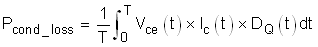
Equation 24. GUID-D9345007-D76B-4A6F-9D22-8B12D457891F-low.gif

where

  • Vce is the conduction voltage drop
  • Ic is the conduction current
  • DQ is the duty cycle
  • T represents one modulation cycle

Switching loss is determined by the switching energy of the device and the switching voltage at a selected test point. Determine the value of the switching energy from the device data sheet using the value of the designed external gate resistor. The remainder of the values needed were determined earlier in the design phase.

Equation 25. GUID-F6792F3C-6626-4934-B420-2D37C818D51B-low.gif

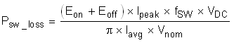
Figure 2-32 shows an example of the graph used to extract the switching energy values from the device data sheet is shown for an C3M0060065D SiC MOSFET.

Figure 2-32 Switching Energy vs Switched Current for C3M0060065D

The diode conduction loss is similarly calculated using known values:
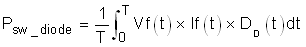
Equation 26. GUID-7A3B6408-AE24-484A-A11A-D51DD5F657CE-low.gif

where

  • Vf is the voltage drop
  • If is the diode current
  • DD is the duty cycle
  • T represents one modulation cycle

Using these three equations, the expected losses of the design are computed for both the SiC MOSFETs as shown in Table 2-1.

Table 2-1 Expected Losses of Switching Devices
PARAMETERC3M0075120D (Q1)C3M0060065D (Q3)
Conduction loss5.76 W4.5 W
Switching loss1.8 W1.13 W
Diode loss0 W0 W
Total7.56 W5.63 W

The final piece of the total system loss estimation is the inductor losses. These losses are determined using the value of the inductor DC and AC resistance and expected inductor current from Section 2.3.1.3.

Equation 27. GUID-1BBFE5E6-038D-4070-AB53-A0F3F69FF197-low.gif
Equation 28. GUID-9EE03A5E-699E-4A15-84E2-7574245FF38F-low.gif

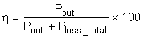
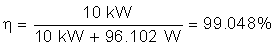
The total major energy loss for this design is then:

Equation 29. GUID-81FD8385-79C3-48DA-A291-F52B66C95030-low.gif
Equation 30. GUID-C24DFDA8-B377-4A49-9BF9-5EB1A60A8ECC-low.gif

Use Equation 30 to determine the total expected inverter efficiency. Note that this is an estimation, but the estimate allows the design to be validated up to this point.

Equation 31. GUID-C7F7AC39-BBB9-420B-80CF-FB62E460E20E-low.gif
Equation 32. GUID-25602919-61ED-4BFA-B349-EE5E3554567D-low.gif