JAJU855 November   2022 TPS51215A


  1.   概要
  2.   リソース
  3.   特長
  4.   アプリケーション
  5.   5
  6. 1System Description
  7. 2System Overview
    1. 2.1 Block Diagram
    2. 2.2 Design Considerations
      1. 2.2.1 DCR current sense
      2. 2.2.2 Subtract and Amplify
      3. 2.2.3 Active Voltage Scale
      4. 2.2.4 IMON Output
    3. 2.3 Highlighted Products
    4. 2.4 System Design Theory
      1. 2.4.1 DCR Current Sense
      2. 2.4.2 Subtract and Amplify
      3. 2.4.3 Active Voltage Scale
      4. 2.4.4 IMON Output
  8. 3Hardware, Software, Testing Requirements, and Test Results
    1. 3.1 Hardware Requirements
    2. 3.2 Test Setup
    3. 3.3 Test Results
      1. 3.3.1 Start-up
      2. 3.3.2 VID Change
      3. 3.3.3 Load Transient
      4. 3.3.4 Load-Line Test
  9. 4Design and Documentation Support
    1. 4.1 Design Files
      1. 4.1.1 Schematics
      2. 4.1.2 BOM
      3. 4.1.3 PCB Layout Recommendations
      4. 4.1.4 Altium Project
      5. 4.1.5 Gerber Files
      6. 4.1.6 Assembly Drawings
    2. 4.2 Documentation Support
    3. 4.3 サポート・リソース
    4. 4.4 Trademarks
  10. 5About the Authors

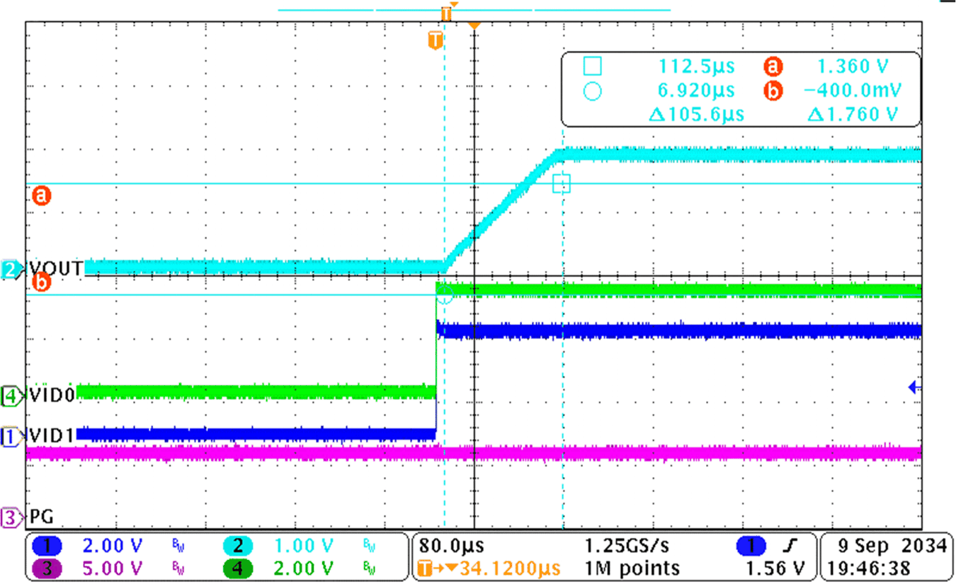
VID Change

Figure 3-3 shows the VID change behavior. VID changes from 00 to 11 and Vout changes from 0 V to 1.8 V.
GUID-20220503-SS0I-HM9Z-FTXZ-WKMZHDFC2VGC-low.png Figure 3-3 VID Change Behavior