SBAA377B April 2022 – January 2024 PCM3120-Q1 , PCM5120-Q1 , PCM6120-Q1 , TLV320ADC3120 , TLV320ADC3140 , TLV320ADC5120 , TLV320ADC5140 , TLV320ADC6120 , TLV320ADC6140
2 Inherent Anti-Aliasing in TLV320ADCx140/TLV320ADCx120/PCMx120-Q1/PCMx140-Q1
TLV320ADCx140/TLV320ADCx120/PCMx120-Q1/PCMx140-Q1 devices use a delta-sigma, analog-to-digital converter to digitize the input signal. The ADC employs over-sampling combined with noise shaping to achieve high performance. Figure 2-1 shows the simplified block diagram of the audio signal chain.
 Figure 2-1 Block Diagram of Audio Signal
Chain
Figure 2-1 Block Diagram of Audio Signal
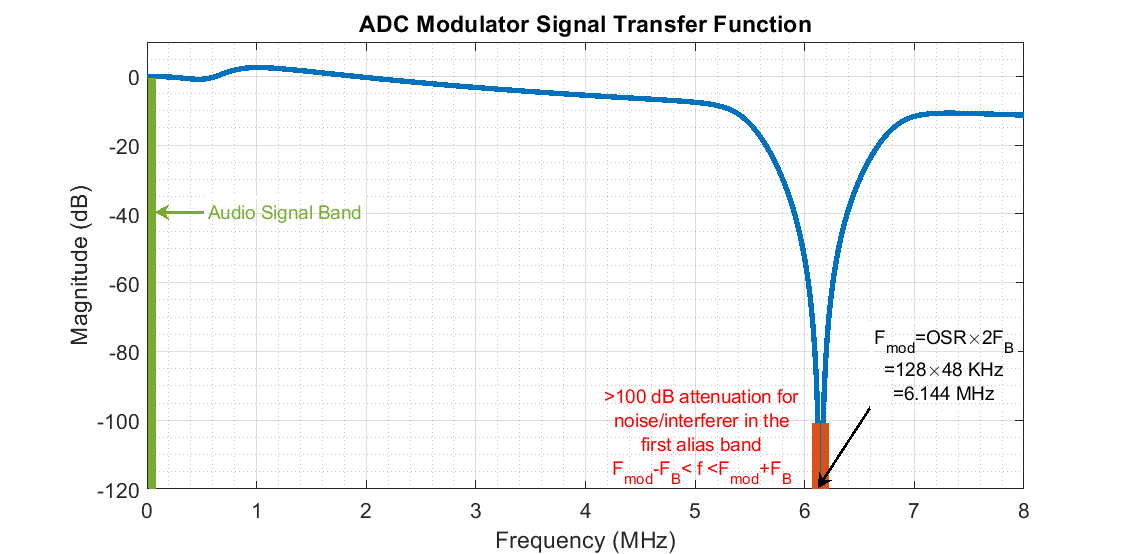
ChainTo improve the performance of the conversion, TLV320ADCx140/TLV320ADCx120/PCMx120-Q1/PCMx140-Q1 not only over-samples the signal to simplify the design of the anti-alias filter, but also adds notches in the signal transfer function at multiples of the modulator frequency (FMOD). The ratio between the sample rate of the modulator and the output sample rate is called the over-sampling ratio (OSR). The frequency bands that can potentially fold into in-band and corrupt the signal of interest are around N×FMOD ±20 kHz (N = 1, 2, 3, and so forth). The notches in the modulator transfer function heavily attenuates (> 100 dB) these frequency bands. Figure 2-2 shows the signal transfer function of the modulator. The sample frequency of the modulator is set to 6.144 MHz for all multiples and sub-multiples of 48 kHz. The 44.1 kHz family of sample rates use a modulator sample frequency of 5.644 MHz. The integrated digital filters, present down the signal chain, cut off the out-of-band frequency noise at every stage of decimation, providing stop band attenuation of more than 70 dB. The overall architecture helps reduce the system cost and overall solution size by getting rid of the on-board operational amplifiers and passives that are required in building a complex high order external analog anti-alias filter.
 Figure 2-2 Signal Transfer Function of
ADC Modulator
Figure 2-2 Signal Transfer Function of
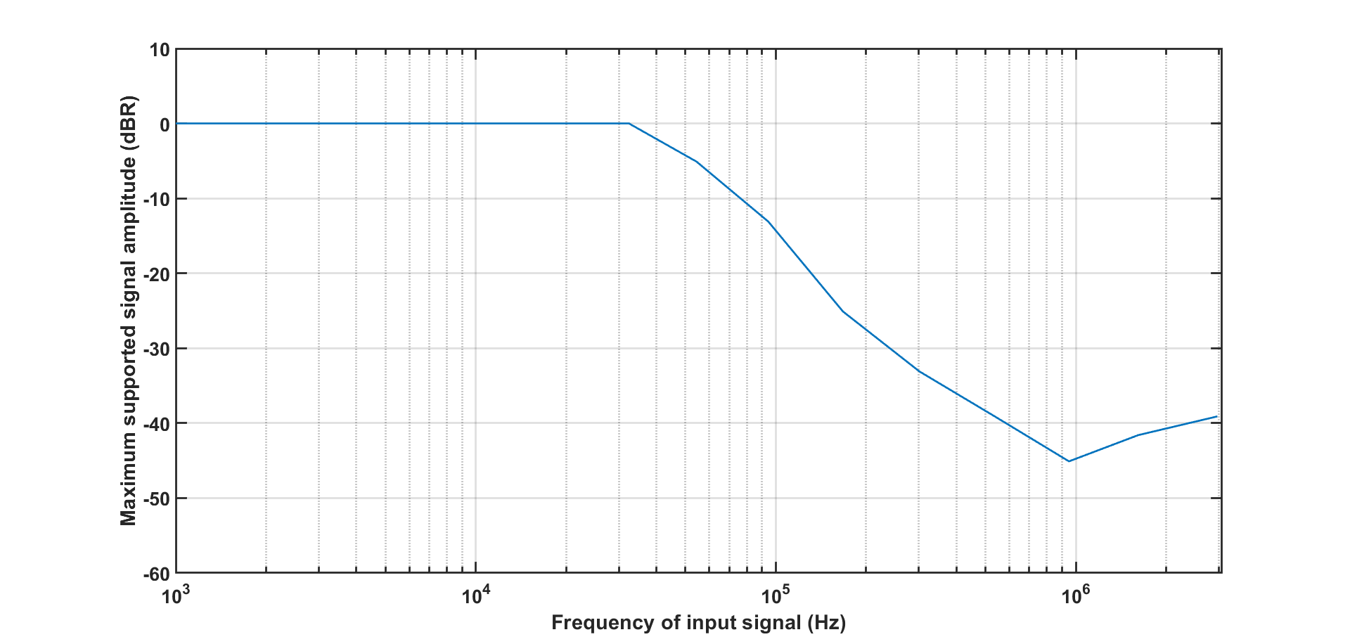
ADC ModulatorThe signal chain in the TLV320ADCx140/TLV320ADCx120/PCMx120-Q1/PCMx140-Q1 devices is tolerant to noise/interferer at the input (no anti-alias required, generally). However, the signal chain cannot sustain noise/interferer above a certain limit. With full scale signal present, the maximum supported integrated noise at the input (entire band) is 0.0075 V (-48 dBr at 2 Vrms). In the absence of signal, the supported value is 0.01 V (-46 dBr at 2 Vrms) of integrated noise. Note that it is assumed that this input noise has a shaped spectrum equivalent to a second order high pass transfer function. For tones (interferer/signal) at specific frequencies, Figure 2-3 shows that the amplitude of the tone can be supported at various frequencies without saturating the modulator.
 Figure 2-3 Maximum Supported Signal
Amplitude
Figure 2-3 Maximum Supported Signal
AmplitudeIf high out-of-band interferer/noise is present, it is recommended it use a first order or second order anti-alias filter with cut off at 20 kHz to keep the out-of-band noise/interferer in check and prevent the signal chain from saturating.